. 2019 Feb 15;5(2):eaau5759.
doi: 10.1126/sciadv.aau5759. eCollection 2019 Feb.

In-memory computing on a photonic platform

Affiliations

In-memory computing on a photonic platform

Carlos Ríos et al. Sci Adv. .

Abstract

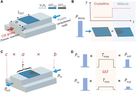
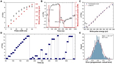
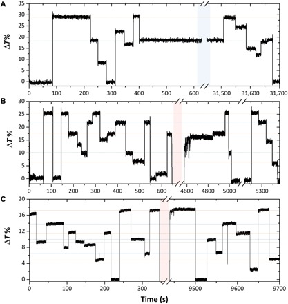
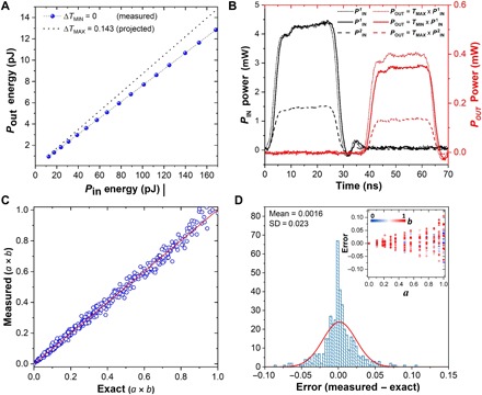
Collocated data processing and storage are the norm in biological computing systems such as the mammalian brain. As our ability to create better hardware improves, new computational paradigms are being explored beyond von Neumann architectures. Integrated photonic circuits are an attractive solution for on-chip computing which can leverage the increased speed and bandwidth potential of the optical domain, and importantly, remove the need for electro-optical conversions. Here we show that we can combine integrated optics with collocated data storage and processing to enable all-photonic in-memory computations. By employing nonvolatile photonic elements based on the phase-change material, Ge2Sb2Te5, we achieve direct scalar and matrix-vector multiplication, featuring a novel single-shot Write/Erase and a drift-free process. The output pulse, carrying the information of the light-matter interaction, is the result of the computation. Our all-optical approach is novel, easy to fabricate and operate, and sets the stage for development of entirely photonic computers.


Figures

Fig. 1
Fig. 1. GST-based photonic memory cell and the scalar multiplication concept.
(A) Scheme of an on-chip bidirectional pump-probe to switch, read, and monitor the transmission in a GST-based nanophotonic memory device. Write and Erase consisted of pulses at λ = 1590 nm and the probe of a low-power CW signal at λ = 1598 nm. LGST = 1 or 2 μm, W = 1.3 μm, and H = 165 nm (etched down from a 330-nm-thick Si3N4). (B) The pulse PWrite is used to switch the GST from a low to a high transmission level, thus defining the transmittance T of the device. (C) Scheme of the multiplication of two scalars a and b, codified in the device transmittance T and in the energy of the read pulse Pin. (D) The low-energy read pulse Pin, which propagates through without inducing phase change, is measured at the output with an amplitude modulated by the transmittance T.
Fig. 2
Fig. 2. Device optimization.
(A) Write pulses with varying widths achieve different transmission levels in a 1-μm-long GST cell before saturating at around 45 ns and their equivalent pulse energy. Shorter pulses can be chosen, thus saving energy and time during memory operations. ΔT = (TTmin)/Tmin is the change in transmission of the level T with respect to the baseline Tmin. (B) Amorphization to a higher transmission level is achieved with a single square Write pulse (13), while a new Erase double-step pulse is used to fully recrystallize, i.e., bring the transmission to the baseline. The latter pulse, at the input, consisted of 14.1 mW (or peak power) for 25 ns and 5.64 mW (0.4 times the peak power) for 100 ns, where peak power is equal to the power used to reach the maximum transmission level. (C) Write pulse energies used for the multilevel conditioning shown in (D) with a linear response by the GST memory cell beyond the threshold energy. (D) Multilevel conditioning of a 2-μm-long GST cell. Thirteen distinguishable levels are demonstrated and accessed randomly; the number of levels is limited only by the SNR and the confidence interval as shown in (E). (E) Error of the multilevel operation calculated from subtracting the measured transmission level from the programmed level in 600 transitions or switching events. The red line corresponds to a normal distribution fitting curve.
Fig. 3
Fig. 3. Drift in transmission.
(A) Multilevel operation of a 2-μm-long GST memory cell using 50-ns pulses with energies in the range of 350 to 600 pJ to Write (upward transitions) and a train of power-decreasing pulses to Erase (downward transitions) level (13). The blue highlighted area corresponds to ~8.5 hours of constant measurement with a CW probe of 0.1 mW (inside the waveguide). (B) Same as (A), but turning the probe OFF for around 1.5 hours. A drift is observed between 4600 and 4800 s, which is corrected by sending the pulse energy of the level where the memory was originally set. (C) Multilevel operation of a different 2-μm-long GST memory cell using 25-ns pulses with energies in the range of 200 to 354 pJ (see Fig. 2D). The Write and Erase were done in the same way as for (A) and (B). The probe was turned off for a time of ~2 hours, but in this case, the CW probe power was reduced to 0.05 mW, which is enough to avoid drift. The colored traces are added to track the evolution of the levels.
Fig. 4
Fig. 4. Scalar multiplication.
(A) Read pulse Pin energies and corresponding measured Pout energy (past the crystalline GST cell and a grating coupler). All the measurements were carried out with the memory cell in the transmission baseline (i.e., ΔT = 0) of the multilevel conditioning shown in Fig. 2C. After each switching, an Erase pulse was used to bring the device to the baseline before the following pulse. A projection of the values for Pout for the case ΔT = 0.143 is plotted for comparison. (B) Demonstration of three multiplications by applying two different Pin, P1in = 112.8 pJ (~4.51 mW for 25 ns) and P2in = 38.9 pJ (~1.56 mW for 25 ns), to memories programmed in the maximum and minimum transmittance levels, ΔT = 0.143 and ΔT = 0, respectively. The result when multiplying by T = 0 corresponds to the level-specific offset. The short time delay between pulses is due to the difference in optical path between the reference pulse and the pulse that is coupled into the photonic chip, both obtained from the pump pulse using a 90/10 beam splitter. (C) Realization of 429, c = a × b multiplications equivalent to 13 different, equally spaced, values for T (reached with PWrite ∈ [180 pJ, 354 pJ]), thus creating 13 values for the multiplicand a, and 33 different values for Pin ∈ [0 pJ, 112.8 pJ] for 33 scalars corresponding to b (note: a, b, c ∈ [0, 1]). PWrite was sent first to establish a level followed by the 33 Pin pulses before changing levels again. (D) Error of the scalar multiplication calculated from subtracting the measured value from the exact. The red line corresponds to a normal distribution fit whose mean and SD values are shown on the plot. The inset corresponds to the error as function of the values of a and b; this shows how for values closer to 1, the error grows linearly, which, in turn, explains the spread for values close to 1 in (C).
Fig. 5
Fig. 5. Photonic architecture for matrix-vector multiplication.
(A) An optical image of the device used to implement multiplication between a 1 × 2 matrix and a 2 × 1 vector is shown on the left. The matrix elements are preprogrammed in the GST (G11 and G12) using two write pulses as discussed in the main text. To implement multiple vectors, pairs of Pin pulses (P1and P2, P3 and P4, etc.) are sent simultaneously and recorded as Pout (P1G11 + P2G12, P3G11 + P4G12, etc.). (B) Change in transmission of the two GST cells as recorded by the probe. Highlighted blue region indicates when PWrite pulses were used to switch one or more GST cells, thus reprogramming the matrix. (C) Recorded traces of input pulses before and after the GST cells. Transmitted power of the optical pulses (dashed lines) is the product of the input pulse and GST’s transmission. (D) Calculated and measured output pulses after combining pulses from the two arms on a photodetector. The different wavelengths in the two arms (1590 and 1598 nm) and linear response of the photodetector ensure that the two multiplied pulses are added together. A factor of ½ is due to the 50% loss at the waveguide splitter.

References

    1. Sun C., Wade M. T., Lee Y., Orcutt J. S., Alloatti L., Georgas M. S., Waterman A. S., Shainline J. M., Avizienis R. R., Lin S., Moss B. R., Kumar R., Pavanello F., Atabaki A. H., Cook H. M., Ou A. J., Leu J. C., Chen Y.-H., Asanović K., Ram R. J., Popović M. A., Stojanović V. M., Single-chip microprocessor that communicates directly using light. Nature 528, 534–538 (2015). - PubMed
    1. Vandoorne K., Mechet P., Van Vaerenbergh T., Fiers M., Morthier G., Verstraeten D., Schrauwen B., Dambre J., Bienstman P., Experimental demonstration of reservoir computing on a silicon photonics chip. Nat. Commun. 5, 3541 (2014). - PubMed
    1. Shainline J. M., Buckley S. M., Mirin R. P., Nam S. W., Superconducting optoelectronic circuits for neuromorphic computing. Phys. Rev. Appl. 7, 034013 (2017).
    1. Shen Y., Harris N. C., Skirlo S., Prabhu M., Baehr-Jones T., Hochberg M., Sun X., Zhao S., Larochelle H., Englund D., Soljačić M., Deep learning with coherent nanophotonic circuits. Nat. Photonics. 11, 441–446 (2017).
    1. D. Kielpinski, R. Bose, J. Pelc, T. Van Vaerenbergh, G. Mendoza, N. Tezak, R. G. Beausoleil, Information processing with large-scale optical integrated circuits, in 2016 IEEE International Conference on Rebooting Computing (ICRC) (2016), San Diego, CA, USA, 17 to 19 October 2016.