. 2019 Feb 22;5(2):eaat8896.
doi: 10.1126/sciadv.aat8896. eCollection 2019 Feb.

Telecom-band lasing in single InP/InAs heterostructure nanowires at room temperature

Affiliations

Telecom-band lasing in single InP/InAs heterostructure nanowires at room temperature

Guoqiang Zhang et al. Sci Adv. .

Abstract

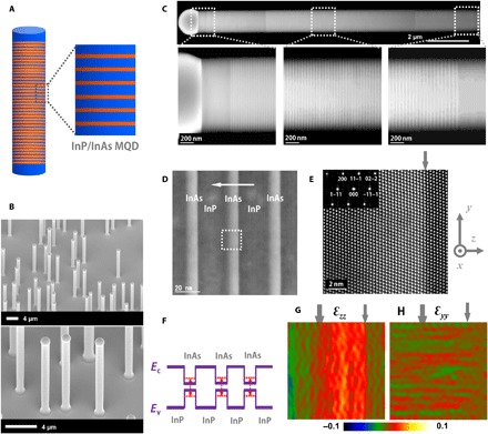
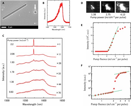
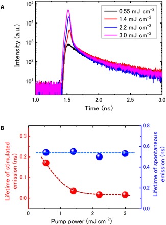
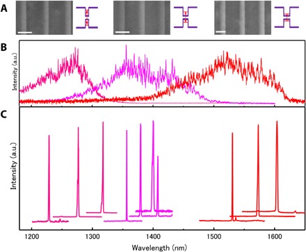
Telecom-band single nanowire lasers made by the bottom-up vapor-liquid-solid approach, which is technologically important in optical fiber communication systems, still remain challenging. Here, we report telecom-band single nanowire lasers operating at room temperature based on multi-quantum-disk InP/InAs heterostructure nanowires. Transmission electron microscopy studies show that highly uniform multi-quantum-disk InP/InAs structure is grown in InP nanowires by self-catalyzed vapor-liquid-solid mode using indium particle catalysts. Optical excitation of individual nanowires yielded lasing in telecom band operating at room temperature. We show the tunability of laser wavelength range in telecom band by modulating the thickness of single InAs quantum disks through quantum confinement along the axial direction. The demonstration of telecom-band single nanowire lasers operating at room temperature is a major step forward in providing practical integrable coherent light sources for optoelectronics and data communication.


Figures

Fig. 1
Fig. 1. InP/InAs MQD nanowires.
(A) Schematic diagram of MQD heterostructure nanowires and magnified view of the heterostructure highlighting the InP/InAs MQD structure. The InAs layer is indicated in red. (B) SEM images (tilt, 38°) of InP/InAs MQD nanowires grown on InP (111)B substrate. A particle can be seen at each nanowire tip. The nanowire diameters are 0.9 to 1.2 μm. The nanowire lengths are 9 to 12 μm. (C) HAADF-STEM images of an InP/InAs MQD nanowire taken along the [011] zone axis. The nanowire contains 400 units of InP/InAs heterostructure. (D and E) Aberration-corrected HAADF-STEM images of InP/InAs heterostructures taken along the [011] zone axis. The horizontal white arrow indicates the growth direction. The thickness of an InAs layer and an InP barrier layer are 9.0 ± 1 and 25.6 ± 1 nm, respectively. The square dotted region in (D) is shown in (E) with high resolution. The dislocation-free InAs/InP interface indicates a coherent growth despite a 3.1% lattice mismatch of InAs/InP. (F) Schematic band diagram of InP/InAs heterostructure nanowires with three InAs QDisks. The thickness as thin as ~9 nm of an InAs QDisk causes quantum confinement effect along the axial direction and thus increases the real gap energy compared with the bulk InAs gap energy (0.36 eV at 300 K), as indicated by red dotted lines. (G and H) Strain mapping of lattice spacing difference along the y and z directions for the STEM image shown in (E), indicating a compressive strain inside the InAs QDisk active region. The gray arrows indicate the InP/InAs interfaces.
Fig. 2
Fig. 2. Optical characterization at room temperature.
(A) SEM image of an InP/InAs MQD nanowire dispersed onto SiO2/Si substrates covered with a 200-nm-thick gold film for optical measurement. The white arrow indicates an indium particle moved from a nanowire tip in mechanical dispersion process. (B) PL spectrum of a single nanowire under a pump laser power of 0.83 mJ cm−2. (C) PL spectra of the nanowire with increasing pump power. The PL intensity continuously increases and eventually a narrow peak appears. Spectra are offset for clarity. (D) Far-field optical image of spatially resolved light emission from individual nanowires with increasing pump power. The diffraction fringes can be seen from the images with pump power of 4.13 mJ cm−2, indicating a lasing action. (E) L-L (light input-output) curve of the excitation power dependence. The curve reveals a transition from spontaneous emission to stimulated emission. The threshold power is estimated to be 2.15 mJ cm−2 per pulse. (F) L-L curve with semi logarithmic axis. Comparison of the measured output power data with a fit derived from the rate equations yields a spontaneous emission factor, β, of 0.0001 to 0.001. The S-shaped curve in the pump power dependence is indicative of the lasing action in the nanowire. a.u., arbitrary units.
Fig. 3
Fig. 3. Time-resolved PL measurements using a single-photon detector with a time resolution of ~16 ps under increasing pump power at room temperature.
(A) The PL decay curves with increasing pump power. For the power higher than 1.4 mJ cm−2, there are two decay times, namely, spontaneous and stimulated emission. (B) Lifetime of spontaneous and stimulated emission under varied pump power. The lifetime of spontaneous emission remains at the same level of 0.5 to 0.54 ns, while the stimulated emission shows faster lifetime with increasing pump power and eventually approaches a constant level of 0.016 ns, which is the resolution of the detector. The error bar is smaller than the dot size. The dashed lines are guides to the eyes. These features confirm the lasing behavior in the nanowire.
Fig. 4
Fig. 4. Tuning the laser wavelength range in telecom band.
(A) Aberration-corrected HAADF-STEM images of InP/InAs MQD nanowires taken along the [011] zone axis. These nanowires were grown with increased flow rates of TMIn:TBA (μmol/min): 0.75:223, 0.98:290, and 1.5:447 from the left-hand side to right-hand side. The flow rates of TMIn:TBA modulate the thickness of the InAs QDisk. From the left-hand side to right-hand side, the thickness of a single InAs QDisk is 6.8 ± 0.8, 7.5 ± 0.8, 9.0 ± 1 nm, respectively. Scale bars, 20 nm. The insets schematically indicate how the real gap energy (ground state) of the InAs QDisk is modulated by the thickness through quantum confinement along the axial direction. (B) Corresponding spontaneous PL spectra of individual nanowires shown in Fig. 4A. The dominant PL peak is shifted up to the high-energy, i.e., short-wavelength, side with decreased flow rates. This indicates enhanced quantum confinement by reduced thickness of a single InAs QDisk. (C) Corresponding PL spectra of stimulated emission. Spectra are offset for clarity. The laser wavelength range is modulated by the growth parameters, i.e., flow rates of TMIn and TBA sources. Thus, a broad wavelength range is covered in the whole telecom band, including two technologically important telecom-band windows of 1.3 and 1.55 μm.

References

    1. Schawlow A. L., Townes C. H., Infrared and optical masers. Phys. Rev. 112, 1940–1949 (1958).
    1. Maiman T. H., Stimulated optical radiation in ruby. Nature 187, 493–494 (1960).
    1. Choquette K. D., Hou H. Q., Vertical-cavity surface emitting lasers: Moving from research to manufacturing. Proc. IEEE 85, 1730–1739 (1997).
    1. Hill M. T., Oei Y.-S., Smalbrugge B., Zhu Y., de Vries T., van Veldhoven P. J., van Otten F. W. M., Eijkemans T. J., Turkiewicz J. P., de Waardt H., Geluk E. J., Kwon S.-H., Lee Y.-H., Nötzel R., Smit M. K., Lasing in metallic-coated nanocavities. Nat. Photonics 1, 589–594 (2007).
    1. Maslov A. V., Ning C.-Z., Size reduction of a semiconductor nanowire laser by using metal coating. Proc. Spie 6468, 64680I (2007).

LinkOut - more resources