Review
. 2018 Feb 9:7:17134.
doi: 10.1038/lsa.2017.134. eCollection 2018.

Electrons dynamics control by shaping femtosecond laser pulses in micro/nanofabrication: modeling, method, measurement and application

Affiliations
Review

Electrons dynamics control by shaping femtosecond laser pulses in micro/nanofabrication: modeling, method, measurement and application

Lan Jiang et al. Light Sci Appl. .

Abstract

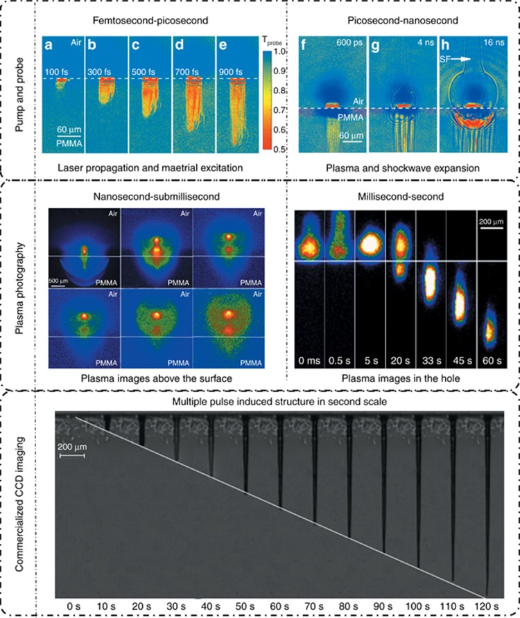
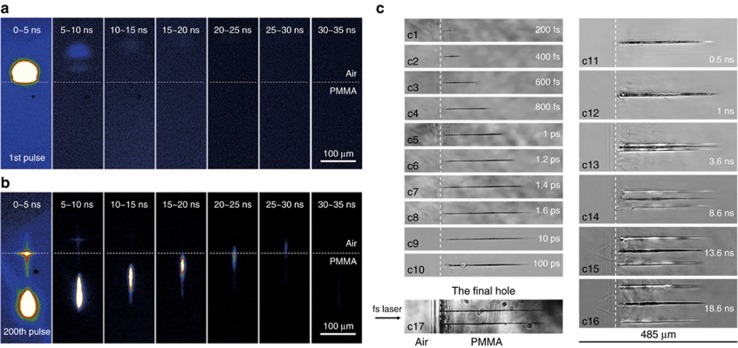
During femtosecond laser fabrication, photons are mainly absorbed by electrons, and the subsequent energy transfer from electrons to ions is of picosecond order. Hence, lattice motion is negligible within the femtosecond pulse duration, whereas femtosecond photon-electron interactions dominate the entire fabrication process. Therefore, femtosecond laser fabrication must be improved by controlling localized transient electron dynamics, which poses a challenge for measuring and controlling at the electron level during fabrication processes. Pump-probe spectroscopy presents a viable solution, which can be used to observe electron dynamics during a chemical reaction. In fact, femtosecond pulse durations are shorter than many physical/chemical characteristic times, which permits manipulating, adjusting, or interfering with electron dynamics. Hence, we proposed to control localized transient electron dynamics by temporally or spatially shaping femtosecond pulses, and further to modify localized transient materials properties, and then to adjust material phase change, and eventually to implement a novel fabrication method. This review covers our progresses over the past decade regarding electrons dynamics control (EDC) by shaping femtosecond laser pulses in micro/nanomanufacturing: (1) Theoretical models were developed to prove EDC feasibility and reveal its mechanisms; (2) on the basis of the theoretical predictions, many experiments are conducted to validate our EDC-based femtosecond laser fabrication method. Seven examples are reported, which proves that the proposed method can significantly improve fabrication precision, quality, throughput and repeatability and effectively control micro/nanoscale structures; (3) a multiscale measurement system was proposed and developed to study the fundamentals of EDC from the femtosecond scale to the nanosecond scale and to the millisecond scale; and (4) As an example of practical applications, our method was employed to fabricate some key structures in one of the 16 Chinese National S&T Major Projects, for which electron dynamics were measured using our multiscale measurement system.

Keywords: electrons dynamics control; femtosecond laser; micro/nano fabrication; pulse shaping.


Conflict of interest statement

The authors declare no conflict of interest.

Figures

Figure 1
Figure 1
The calculated electron and phonon temperatures of 200 nm gold film irradiated by a 140 fs, 1053 nm pulse at 0.2 J cm−2 by (a) the classical model and (b) the improved model. (c) The predicted damage threshold fluences of 200 nm gold film processed by a 1053 nm laser at different pulse. Reproduced from Ref. (with the permission of SPIE).
Figure 2
Figure 2
Schemes of electrons dynamics adjusted by shaped femtosecond laser pulses. Electric fields of the applied laser pulse and time-dependent excited electrons of diamond with different (a) pulse delays and (b) sub-pulse numbers. (c) Electric fields of the applied laser pulse (top panel) and the electron density change of diamond from that in the ground state after laser termination with different pulse energy ratios. (d) Time-dependent electron temperature of fused silica with different pulse dual-wavelengths. Reproduced from Ref. (with the permission of IOP) and Ref. (with the permission of AIP publishing).
Figure 3
Figure 3
Simulation of materials properties adjusted by varying pulse delay within a femtosecond laser pulse train. (ae) Reflectivity of the material surface and (fj) the corresponding peak laser intensity distribution at different pulse delays.
Figure 4
Figure 4
Schemes of phase change controlled by varying the pulse delay in a fs pulse train. Snapshots of nickel thin films irradiated by femtosecond laser (ad) single pulse and (eh) 20 pulse trains with the total fluence of 0.28 J cm−2, where X is in the direction of Ni (100) surface and Z is in the direction of laser irradiance. Lattice temperature and stress distributions at different times for (i and k) the single pulse and (j and l) the 20 pulse trains. Time evolution of the system in the ρ-T plane for different regions for (m and n) the single pulse and (o and p) the 20 pulse trains. Arrows indicate the time evolution. Reproduced from Ref. (with the permission of AIP publishing).
Figure 5
Figure 5
Schemes of ablation crater shape controlled by shaped femtosecond laser pulse, , . (a) Ablation crater shapes created by femtosecond pulse trains consisting of double pulses with different pulse delays at a total fluence of 5 J cm−2 and central wavelength of 780 nm. (b) Ablation crater shapes created by femtosecond laser pulse trains with different wavelength composition at the total fluence of 5.0 J cm−2 and the pulse delay of 50 fs. (c) Ablation crater shapes created by 800 nm femtosecond pulse trains consisting of double pulses with three different energy ratios at the pulse delay of 50 fs. Reproduced from Ref. (with the permission of IOP), 111 (with the permission of AIP publishing) and 112 (with the permission of Springer).
Figure 6
Figure 6
Temporally shaping femtosecond pulses: (a) a conventional femtosecond pulse is temporally shaped into a pulse train; (b) the number of sub-pulses within a train can be controlled; (c) the delay between sub-pulses can be controlled; (d) the energy ratio of sub-pulses can be controlled.
Figure 7
Figure 7
Schematic of the experimental setup for temporal shaping of femtosecond pulses. Reproduced from Ref. (with the permission of Springer).
Figure 8
Figure 8
Holes machined using (a) five 355-nm nanosecond pulses (duration of 30 ns, energy of 0.16 μJ), (b) five 800-nm femtosecond pulses (duration of 120 fs, energy of 0.12 μJ), (c) five femtosecond-nanosecond pulse pairs, (d) an 800 nm femtosecond laser double-pulse train (duration of 50 fs, energy of 20 μJ) . Reproduced from Ref. (with the permission of OSA) and Ref. (with the permission of OSA).
Figure 9
Figure 9
Morphology evolution of the sample surface exposed by (ae) a femtosecond laser single pulse; (fj) femtosecond laser double pulses at different stages of the etching process, the pulse delay is 350 fs. The SEM images have varying scale bars. (kn) Simulation of the free electron density distributions and (or) center laser intensity distributions in fused silica irradiated by femtosecond double pulses at different pulse delays. (s) Schematic diagram of the manufacturing and Si-O bond structure. (t) Normalized Raman spectra of modified regions irradiated using femtosecond laser single and double pulses (the pulse delay is 350 fs) in fused silica. Dashed lines below the D2 peaks are baselines used in the peak area measurement in u. Inset is the schematic diagram of 4- and 3-membered ring structures. (u) Percent area of the total reduced Raman spectrum under the D2 line versus different pulse delays. The femtosecond laser with wavelength of 800 nm, duaration of 50 fs and repetition rate up to 1 KHz. The laser fluence is fixed at 9.46 J cm−2 in all experiments and the energy distribution ratio is 1:1. Reproduced from Ref. (with the permission of NPG).
Figure 10
Figure 10
Control of period, orientation and topology of the LIPSS on the surface of fused silica via symmetrically shaped femtosecond pulses. (ah) LSFL changes to HSFL with different orientation under certain pulse fluences and pulse delays on fused silica. (io) SEM images of representative HSFL (ik), LSFL (mo) and double-grating structure (l) on fused silica for single-pulse trains (Ns=1), double-pulse trains (Ns=2), triple-pulse trains (Ns=3) and quadruple-pulse trains (Ns=4), respectively. Reproduced from Ref. (with the permission of OSA) and Ref. (with the permission of OSA).
Figure 11
Figure 11
(ae) One-step method fabrication of controllable SERS substrates. (a and b) SEM images of the silicon irradiated at pulse delays of 0 fs, and 800 fs, respectively. (c) Size distribution of silver nanoparticles in a (black), and b (red). (d) SERS signals of R6G molecules on the as-prepared substrates at various pulse delay. (e) Enhancement factors with different pulse delays. (fk) Two-step method fabrication of controllable SERS substrate. f Schematic diagram of the SERRS substrate fabrication process. (gj) SEM images of silicon substrates irradiated at pulse delays of g 0 fs, and i 1000 fs in deionized water, (h) 0 fs and (j) 1000 fs in 10-mM silver nitrate solution. (k) SERS spectrum of substrates fabricated at different pulse delays. Reproduced from Ref. (with the permission of OSA), and Ref. (with the permission of OSA).
Figure 12
Figure 12
Morphology evolution of gold NPs reduced on MoS2 surfaces irradiated by femtosecond (ad) single and (eh) double pulses, at different stages of the reduction process, where tr represents the chemical reduction time, the pulse delay is 5 ps. (i) Schematic diagram of the manufacturing and Mo-S bond structure. XPS S 2p spectra of modified regions irradiated by femtosecond laser (j) double and (k) single pulses on MoS2, where the percentage value represents the content of unbound sulfur and the atomic ratio represents the relative atomic concentration ratio of Mo and S atoms. (l) AFM image and (m) atomic scale schematic of the laser-broken micro/nano MoS2 debris. (n) Mechanism of chemical reduction of gold cations on laser-treated MoS2 (Ref. 127). Reproduced from Ref. (with the permission of ACS).
Figure 13
Figure 13
(a) Dependence between the recast ratio (recast area/ablation area) and pulse delay on fused silica fabrication using femtosecond laser pulse trains consisting of two identical sub-pulses with an identical total fluence. AFM profiles of the structures of the fused silica fabrication using (b) a conventional single pulse and (c) femtosecond laser pulse train with a pulse delay of 300 fs. SEM images of the structures on fused silica fabrication using a femtosecond laser pulse train with different energy ratios between the two sub-pulses: (d) 1:1 and (e) 2:1. The femtosecond laser with wavelength of 800 nm, duration of 35 fs and repetition rate up to 1 KHz. The total fluence of the pulse trains in all experiments is 5 J cm−2; the scale bar in d and e is 500 nm. Reproduced from Ref. (with the permission of OSA).
Figure 14
Figure 14
Shaping conventional Gaussian beam into different beam types.
Figure 15
Figure 15
Schematic diagram of the experimental setup. WS: white light source; BS: beam splitter; DM: dichroic mirror; L1, L2: two convex lenses consisting of a 4f relay system; L3: convex lens; Inset: section of the samples and the focusing laser in the yz plane. Reproduced from Ref. (with the permission of Wiley).
Figure 16
Figure 16
Fabrication of nanowire by spatial pulse shaping. (a) Single spot fabricated by the shaped beam. (b) Scanning electron microscope (SEM) images of nanowire. (c and d) AFM images of the nanowire and its cross section. (e) EDXS measurements of the metal nanowire and the ablation area. (f) Five-ring patterns fabricated by the proposed methods. Reproduced from Ref. (with the permission of Wiley).
Figure 17
Figure 17
Testing of the resistivity of the nanowire. (a) The SEM images of the nanowire and the electrode pads. (b) The volt-ampere characteristics of the nanowires. Reproduced from Ref. (with the permission of Wiley).
Figure 18
Figure 18
Schematic of multiscale measurement of femtosecond laser drilling, including laser propagation and laser-induced material excitation, plasma and shockwave evolution and hole formation and so on. (a) Pump-probe shadowgraph imaging technique. (b) Laser-induced breakdown spectroscopy (LIBS). (c) Time-resolved plasma photography with gated intensified charge-coupled device (ICCD). (d) Industrial continuous imagery.
Figure 19
Figure 19
Multiscale measurement results of deep-hole drilling process in PMMA. Multiscale measurement results of deep-hole drilling process in PMMA with 100 μJ pulse energy focused by plano-convex lens (f=100 mm). The dynamics include femtosecond-picosecond electron excitation, picosecond–nanosecond plasma and shockwave evolution and multiple pulse-induced structure in second scale.
Figure 20
Figure 20
Typical spectra of PMMA plasma irradiated by a single pulse and a double pulse with the same total fluence of 7.8 J cm−2. Reproduced from Ref. (with the permission of SPIE).
Figure 21
Figure 21
Characterizations of femtosecond laser double pulse induced plasma of fused silica (a) plasma images, (b) electron densities and (c) plasma temperature.
Figure 22
Figure 22
(a) Schematic of the spatial shaping femtosecond laser pulses microdrilling setups; (b) Morphology images of microholes drilled with a single pulse Bessel beam and Gaussian beam, respectively; (c) Intensity distribution simulations of the Bessel beam and Gaussian beam; (d) The hollowness characterization of microholes drilled by single-pulse Bessel beam. Reproduced from Ref. (with the permission of Springer).
Figure 23
Figure 23
Time-resolved images of the plasma expansion during the Gauss beam drilling for the 1st pulse (a) and 200th pulse (b), respectively, pump-probe shadowgraph study (c) of Bessel beam drilling. c1–c16 Time-resolved images of femtosecond-picosecond-nanosceond dynamics of Bessel beam drilling. c17 The final hole morphology drilled by Bessel beam. Reproduced from Ref. (with the permission of OSA) and Ref. (with the permission of OSA).
Figure 24
Figure 24
(a and b) The image of a microhole array throughout a 1 cm × 1 cm large area using the flying punch method for Bessel beam; (c) the local magnified OTM image of a microhole array; (d) the local magnified OTM image of microholes in the central array under 100 × microscope objective. Reproduced from Ref. (with the permission of Springer).

References

    1. Malinauskas M, Žukauskas A, Hasegawa S, Hayasaki Y, Mizeikis V et al. Ultrafast laser processing of materials: from science to industry. Light Sci Appl 2016; 5: e16133 doi:10.1038/lsa.2016.133.. - PMC - PubMed
    1. Sugioka K, Cheng Y. Ultrafast lasers—reliable tools for advanced materials processing. Light Sci Appl 2014; 3: e149 doi:10.1038/lsa.2014.30..
    1. Gamaly EG. Femtosecond Laser-Matter Interaction: Theory, Experiments and Applications. Boca Raton: CRC Press; 2011.
    1. Levis RJ, Menkir GM, Rabitz H. Selective bond dissociation and rearrangement with optimally tailored, strong-field laser pulses. Science 2001; 292: 709–713. - PubMed
    1. Rezaei S, Li JZ, Herman PR. Burst train generator of high energy femtosecond laser pulses for driving heat accumulation effect during micromachining. Opt Lett 2015; 40: 2064–2067. - PubMed