. 2019 Feb;15(2):127-131.
doi: 10.1038/s41567-018-0328-0. Epub 2018 Nov 12.

Design and characterization of electrons in a fractal geometry

Affiliations

Design and characterization of electrons in a fractal geometry

S N Kempkes et al. Nat Phys. 2019 Feb.

Abstract

The dimensionality of an electronic quantum system is decisive for its properties. In one dimension electrons form a Luttinger liquid and in two dimensions they exhibit the quantum Hall effect. However, very little is known about the behavior of electrons in non-integer, or fractional dimensions1. Here, we show how arrays of artificial atoms can be defined by controlled positioning of CO molecules on a Cu (111) surface2-4, and how these sites couple to form electronic Sierpiński fractals. We characterize the electron wave functions at different energies with scanning tunneling microscopy and spectroscopy and show that they inherit the fractional dimension. Wave functions delocalized over the Sierpiński structure decompose into self-similar parts at higher energy, and this scale invariance can also be retrieved in reciprocal space. Our results show that electronic quantum fractals can be artificially created by atomic manipulation in a scanning tunneling microscope. The same methodology will allow future study to address fundamental questions about the effects of spin-orbit interaction and a magnetic field on electrons in non-integer dimensions. Moreover, the rational concept of artificial atoms can readily be transferred to planar semiconductor electronics, allowing for the exploration of electrons in a well-defined fractal geometry, including interactions and external fields.


Conflict of interest statement

Authors declare no competing interest.

Figures
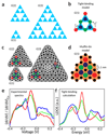
Figure 1
Figure 1. Geometry of the Sierpiński triangle fractal.
a, Schematic of Sierpiński triangles of the first three generations G(1)-G(3). G(1) is an equilateral triangle subdivided in four identical triangles, from which the center triangle is removed. Three G(1) (G(2)) triangles are combined to form a G(2) (G(3)) triangle. b, Geometry of a G(1) Sierpiński triangle with red, green and blue atomic sites. t and t′ indicate nearest-neighbor and next-nearest-neighbor hopping between the sites in the tight-binding model. c, Constant-current STM images of the realized G(1)-G(3) Sierpiński triangles. The atomic sites of one G(1) building block are indicated as a guide to the eye. Imaging parameters: I = 1 nA, V = 1 V for G(1) – G(2) and 0.30 V for G(3). Scale bar, 2 nm. d, The configuration of CO molecules (black) on Cu(111) to confine the surface-state electrons to the atomic sites of the Sierpiński triangle. e, Normalized differential conductance spectra acquired above the positions of red, blue and green open circles in c (and equivalent positions). f, LDOS at the same positions, simulated using a tight-binding model with t = 0.12 eV, t′ = 0.01 eV and an overlap s = 0.2.
Figure 2
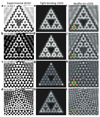
Figure 2. Wave-function mapping.
a-d, Differential conductance maps acquired above a G(3) Sierpiński triangle at bias voltages −0.325 V, −0.200 V, −0.100 V, and +0.100 V. Scale bar: 5 nm. e-h, LDOS maps at these energies calculated using the tight-binding model. i-l, LDOS maps simulated using the muffin-tin approximation. As a guide to the eye, a G(1) building block is indicated, in which a larger radius of the circles corresponds to a larger LDOS at an atomic site, while no circle indicates a node in the LDOS.
Figure 3
Figure 3. Fractal dimension of the Sierpiński wave-function maps.
a, The box-counting dimension of the wave-function map acquired at V = −0.325 V is obtained from the slope of log(N) vs. log(r−1). The magenta dot indicates the radius r of the N circles used in the inset. Inset: Schematic of the box-counting method, where N circles with radius r cover the contributing experimental LDOS above the threshold of 45% at V = −0.325 V (see Supplementary Information for the determination of this threshold). b, Determination of the fractal dimensions of the LDOS of the G(3) Sierpiński triangle (orange) and comparison with the 2D square lattice from Ref. (blue) for the experimental (dark) and muffin-tin (light) wave function maps. The solid lines indicate the geometric Sierpiński Hausdorff dimension (D = 1.58) and that of the square lattice (D = 2). The error bars display the maximum of the error in determining the fractal dimension at different LDOS thresholds, which is between 45% - 65% (60% - 90%) for experiment (muffin-tin)) and the error in determining the slope of the loglog plot as seen in a. The green result at −0.325 V is obtained from the slope in a. The fluctuations in the dimension are caused by nodes in the LDOS maps at different energies.
Figure 4
Figure 4. Fourier analysis of wave-function maps.
a, Fourier transform of the experimental differential conductance map at −0.325 V. The k-values outside the circles are excluded from the Fourier-filtered images in b-d. Scale bar: k = 3 nm−1. b-d, Wave-function map at −0.325 V after Fourier-filtering, including merely the k-values within the turquoise (b), red (c), and yellow (d) circles indicated in a. Scale bar: 5 nm.

References

    1. Mandelbrot BB. In: The Fractal Geometry of Nature. Freeman WH, editor. 1982.
    1. Gomes KK, Mar W, Ko W, Guinea F, Manoharan HC. Designer Dirac fermions and topological phases in molecular graphene. Nature. 2012;483:306–310. - PubMed
    1. Slot MR, et al. Experimental realization and characterization of an electronic Lieb lattice. Nature Physics. 2017;13:672–676. - PMC - PubMed
    1. Collins LC, Witte TG, Silverman R, Green DB, Gomes KK. Imaging quasiperiodic electronic states in a synthetic Penrose tiling. Nature Communications. 2017;8:15961. - PMC - PubMed
    1. Newkome GR, et al. Nanoassembly of a Fractal Polymer: A Molecular ”Sierpinski Hexagonal Gasket”. Science. 2006;312:1782–1785. - PubMed