. 2018 Jul;2(7):508-521.
doi: 10.1038/s41551-018-0230-1. Epub 2018 Apr 30.

Rational design of silicon structures for optically controlled multiscale biointerfaces

Affiliations

Rational design of silicon structures for optically controlled multiscale biointerfaces

Yuanwen Jiang et al. Nat Biomed Eng. 2018 Jul.

Abstract

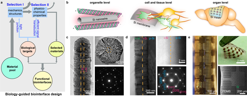
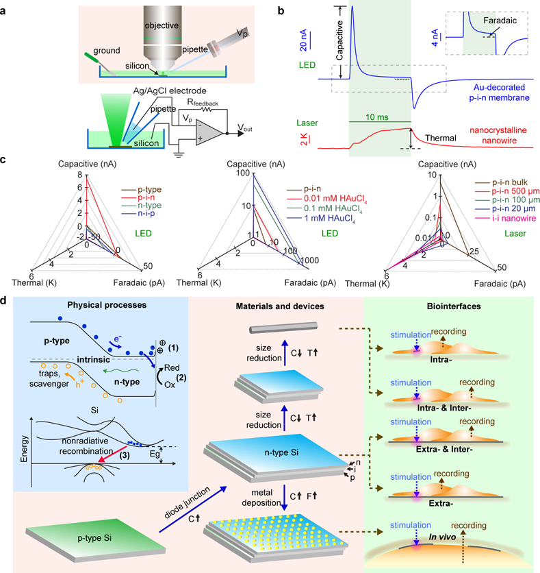
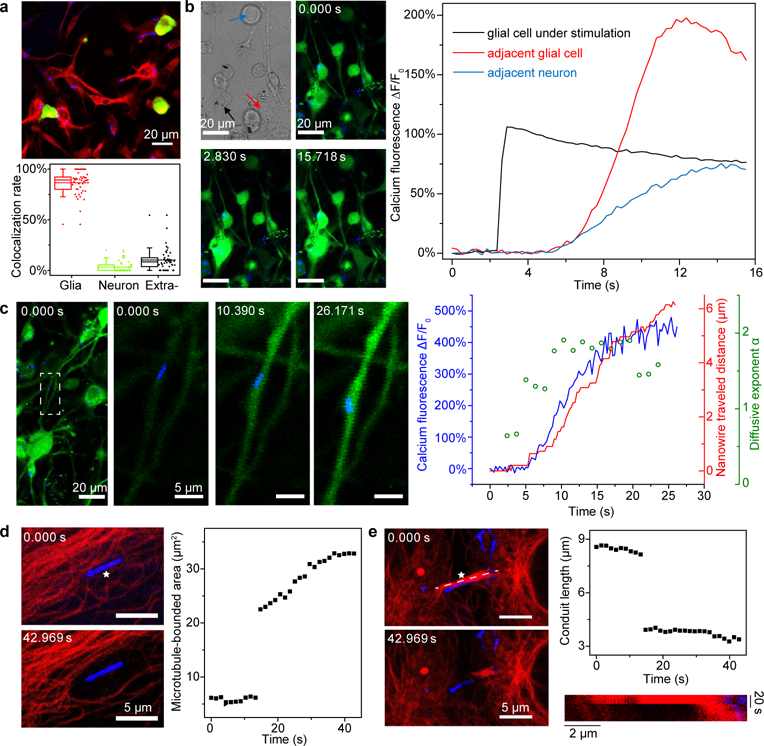
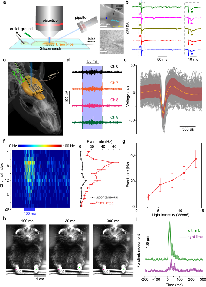
Silicon-based materials have been widely used. However, remotely controlled and interconnect-free silicon configurations have been rarely explored, because of limited fundamental understanding of the complex physicochemical processes that occur at interfaces between silicon and biological materials. Here, we describe rational design principles, guided by biology, for establishing intracellular, intercellular and extracellular silicon-based interfaces, where the silicon and the biological targets have matched properties. We focused on light-induced processes at these interfaces, and developed a set of matrices to quantify and differentiate the capacitive, Faradaic and thermal outputs from about 30 different silicon materials in saline. We show that these interfaces are useful for the light-controlled non-genetic modulation of intracellular calcium dynamics, of cytoskeletal structures and transport, of cellular excitability, of neurotransmitter release from brain slices, and of brain activity in vivo.


Conflict of interest statement

Code availability Custom codes used to analyze the data are available upon reasonable request to the corresponding author. Competing financial interest The authors declare no competing financial interests.

Figures

Figure 1 |
Figure 1 |. Si structures for multiscale biointerfaces.
a, A schematic diagram illustrating the principle of biology-guided biointerface design. The intended biological targets place selection criteria for material structure (I) and function (II), so that the selected materials would display a better chance to establish functional biointerfaces. b, Silicon-based materials, e.g., nanowires (left), thin membranes (middle), and distributed meshes (right), are chosen after Selection I to form tight interfaces with various biological targets, spanning multiple length scales, e.g., organelles (left), single cells or small tissues (middle), and organs (right). c, An intrinsic-intrinsic coaxial Si nanowire is synthesized from the deposition of a thick shell over a thin VLS-grown nanowire backbone as shown in a side-view TEM image (left). A cross-sectional TEM image (upper right) shows diameters of ~ 50 nm and ~ 270 nm for the core and shell, respectively. A corresponding SAED pattern (lower right) confirms the nanocrystalline structure. Orange dashed lines highlight the core/shell boundaries. d, A multilayered p-i-n Si diode junction made by a CVD synthesis of intrinsic (magenta) and n-type (green) Si layers onto a p-type (cyan) Si SOI substrate. A cross-sectional TEM image (left) shows the columnar structures of the intrinsic and n-type layers. A low-angle annular dark field scanning TEM (LAADF STEM) image (upper right) and a SAED (zone axis B = [011], lower right) pattern taken at the p-type (cyan)/intrinsic (magenta) interface both highlight the single crystalline p-type layer (isolated spots (blue) from SAED, periodic atomic columns from STEM) and the nanocrystalline intrinsic layer (concentric rings (magenta) from SAED, small crystal domains from STEM). A sharp and oxide free interface is evident from the STEM image with a junction width of < 1 nm. Orange dashed lines mark the intrinsic/n-type (left) and the p-type/intrinsic (upper right) interfaces. e, A flexible device composed of a stack of a distributed Si mesh and a holey PDMS membrane. The flexibility is demonstrated by optical (left) and scanning electron (lower right) micrographs and a photograph (upper right) taken from the same device under rolling or bending.
Figure 2 |
Figure 2 |. Photo-responses of Si materials.
a, Schematic diagrams illustrating the experimental setup for the photo-response measurements from Si structures. Light pulses (530 nm LED or 532 nm laser) are delivered through a water-immersion objective to the Si submerged in a PBS solution. Light-induced currents are recorded at different pipette command potentials (Vp) using a voltage-clamp mode, from which capacitive, Faradaic and thermal components can be either directly measured or derived by mathematic fitting. b, Representative photo-responses of an Au-decorated p-i-n Si diode junction (top, from 1 mM HAuCl4, LED illumination, ~ 12.05 mW, ~ 500 μm spot size, ~ 6 W/cm2) and an i-i nanocrystalline nanowire (bottom, laser illumination, 47.1 mW, ~ 5 μm spot size, ~ 240 kW/cm2) showing three major types of the responses, i.e., capacitive (upper), Faradaic (upper inset), and thermal (lower). LED-induced capacitive and Faradaic currents are pronounced in the Au-decorated diode junction. The capacitive current is defined as the maximal current amplitude reached after the light onset while the Faradaic current is defined as the current amplitude at the time point of 8.5 ms since illumination starts. The nanocrystalline nanowire generate significant heating of the surrounding PBS via its photothermal effect under laser illumination. Green shaded areas highlight the light illumination periods. The grey dashed box marks the region for the inset. c, Quantitative matrices of the three photo-responses, used to evaluate the impact of important materials parameters, e.g., doping (left), surface chemistry (middle), and size (right). Diode junctions (left, p-i-n and n-i-p) show significantly enhanced capacitive currents versus uniformly doped SOI substrates (p-type and n-type). Au-decorated p-i-n diode junctions (middle) promote both capacitive and Faradaic currents. Si structures with smaller dimensions (right) show stronger photothermal responses. d, A principle for Selection II (Fig. 1a), highlighting the physical origins (light blue block), the material developing pathways (light orange block), and the projected biointerfaces (light green block). Fundamental processes include the accumulation of ions to balance light-generated excessive carriers near Si surface (1, capacitive, C), the metal-mediated redox reactions (2, Faradaic, F), and the thermalization through phonon emission (3, thermal, T). Considering the size and mechanics match at the biointerfaces (i.e., Selection I, Fig. 1a), these Si structures can be utilized to form optically-controlled intra- (Si nanowires), inter- (Si nanowires and p-i-n diode junctions), and extra-cellular (pristine and metal-decorated p-i-n diode junctions) biointerfaces.
Figure 3 |
Figure 3 |. Si nanowire-enabled intracellular stimulation interfaces.
a, A confocal microscope image (top) of a DRG-nanowire coculture shows the cell-type-specific overlapping of Si nanowires (green, neurons; red, glial cells; blue, Si nanowires). Statistical analysis of the nanowire-cell colocalization rate (bottom) reveals that ~ 87% of total nanowires overlap with glial cells, ~ 3% with neurons, and ~ 10% stay in the extracellular space. Half of the data points are within the boxes, 80% are within the whiskers. Solid and dashed lines represent the medians and means, respectively. Round dots mark the maximum and minimum values. Diamond dots represent the raw data points. Statistics are from images taken from 45 regions of 3 different cultures. b, Confocal microscope time series images (upper middle, lower left, and lower middle; green, calcium; blue, Si nanowires) show that a glial cell with an internalized nanowire can be optically stimulated to trigger intracellular calcium elevation and subsequent intercellular calcium wave propagations to both glial cells and neurons. A differential interference contrast (DIC) image (upper left) highlights the nanowire under stimulation (black arrow) and the morphologies of a neighboring glial cell (red arrow) and a neuron (blue arrow). The laser illumination (592 nm, ~ 14.4 mW) was on for 1 ms right before the time point of 2.830 s. Quantitative analysis of the fluorescence intensities over time (right) from three regions of interest show calcium dynamics in all cells (black, the glial cell being stimulated; red, a nearby glial cell; blue, a neighboring neuron). c, Si nanowires can serve as a dual-role intracellular biophysical tool, i.e., a calcium modulator and a marker for motor protein-microtubule interactions. The location of a nanowire (i.e., a transport marker) in a glial protrusion is tracked while the nearby calcium dynamics is monitored simultaneously, following a remote laser illumination of a different nanowire (i.e., a calcium modulator) to initiate a calcium flux within the network (green, calcium; blue, Si nanowires; first one from left). The white dashed box marks the region of interest for the transport study. Time series images (second one from left, middle one, second one from right) show a calcium-correlated motion of the Si nanowire. MSD analysis further suggests a mode shift of the nanowire motion from random or restricted diffusions (rolling MSD diffusivity exponent, α ≤ 1) to an active transport (α ~2). d, Microtubule networks can be mechanically manipulated by laser illumination (592 nm, 1 ms, ~ 2.09 mW) of intracellular Si nanowires. Red, microtubules; blue, Si nanowires. The white star marks the illumination site on the nanowire. e, Intercellular conduits can also be manipulated (592 nm, 1 ms, ~ 2.55 mW). Red, microtubules; blue, Si nanowires. A kymograph (lower right) taken along the white dashed line (upper left) shows the evolution of the conduit length. The white star marks the illumination site on the nanowire.
Figure 4 |
Figure 4 |. Flexible and distributed silicon mesh for optically-controlled extracellular neuromodulation.
a, A schematic diagram of a photostimulation of a brain slice performed in a perfusion chamber (left). A pyramidal neuron in a cortex slice was held at −70 mV in the whole-cell voltage-clamp mode (lower right) while a distributed Si mesh was placed underneath the slice (upper right). Short laser pulses (473 nm, 1 ms, ~ 2 mW, ~ 57 μm spot size) were delivered to a spot on the Si mesh (marked by a blue star) to activate the nearby cells. b, Example traces from voltage clamp recordings of the patched pyramidal neuron over 5 trials (left) with 1-ms long laser stimulations (cyan bar). The grey dashed box marks the time frame for zoom-in views on the right. EPSCs are marked by stars following the illuminations of the Si mesh (right). The cyan shaded area marks the illumination period in each trial. # denotes the photoelectric artifact. c, A schematic diagram illustrating the in vivo photostimulation test. A linear probe with 32 recording sites is guided into a head-fixed anesthetized mouse brain to sample the evoked neural activities by the illumination of an adjacent silicon mesh. d, Example traces of raw neural response data from four adjacent channels (Ch 6 to Ch 9) in a single trial of stimulation (473 nm, 100 ms, ~ 5 mW, ~216 μm spot size) marked by a light blue band. e, A mean neuron-firing waveform (orange) superposed on individual waveforms (black) of both spontaneous and stimulation-evoked activities. The maroon shaded area denotes standard deviations. Data are from 300 waveforms, with 153 from stimulated events and 147 from spontaneous events, in one representative photostimulation experiment on one mouse. f, A heat map of PSTH for channels between 4 and 19 (left) and the mean spontaneous and evoked neural response rates across all trials for the same channels in the PSTH heat map (right). The blue bar underneath the heat map indicates the period of laser stimulation. Error bars denote standard error of the mean (s.e.m.) of the data from 50 trials in one representative photostimulation experiment on one mouse. g, The evoked mean neural response rate is positively correlated with the stimulation laser intensity. Error bars represent s.e.m. from 50 trials in channel 9 in one representative photostimulation experiment on one mouse. h, Snapshots of a forelimb movement study following photostimulations. The mouse’s left limb (green dot) moves up and down following the laser illumination (473 nm, 50 ms, ~ 4 mW, ~ 216 μm spot size) on a Si mesh attached to the right side of the forelimb primary motor cortex. See Supplementary Video 1 for more details. i, Time-dependent mean limb movements show a preferred motion of the left forelimb after the stimulation. The 0 ms time point represents the start of the light pulse. Shaded areas denote s.e.m. of the data. Data are from 15 trials in one representative photostimulation experiment on one mouse.

Comment in

  • Silicon biointerfaces for all scales.
    Park S, Frank JA, Anikeeva P. Park S, et al. Nat Biomed Eng. 2018 Jul;2(7):471-472. doi: 10.1038/s41551-018-0268-0. Nat Biomed Eng. 2018. PMID: 30948826 No abstract available.

References

    1. Viventi J, Kim DH, Vigeland L, Frechette ES, Blanco JA, Kim YS, Avrin AE, Tiruvadi VR, Hwang SW, Vanleer AC, Wulsin DF, Davis K, Gelber CE, Palmer L, Van der Spiegel J, Wu J, Xiao J, Huang Y, Contreras D, Rogers JA & Litt B Flexible, foldable, actively multiplexed, high-density electrode array for mapping brain activity in vivo. Nature Neuroscience 14, 1599–1605, 10.1038/nn.2973 (2011). - DOI - PMC - PubMed
    1. Tian B, Cohen-Karni T, Qing Q, Duan X, Xie P & Lieber CM Three-dimensional, flexible nanoscale field-effect transistors as localized bioprobes. Science 329, 830–834, 10.1126/science.1192033 (2010). - DOI - PMC - PubMed
    1. Liu J, Fu TM, Cheng Z, Hong G, Zhou T, Jin L, Duvvuri M, Jiang Z, Kruskal P, Xie C, Suo Z, Fang Y & Lieber CM Syringe-injectable electronics. Nature Nanotechnology 10, 629–636, 10.1038/nnano.2015.115 (2015). - DOI - PMC - PubMed
    1. Chiappini C, De Rosa E, Martinez JO, Liu X, Steele J, Stevens MM & Tasciotti E Biodegradable silicon nanoneedles delivering nucleic acids intracellularly induce localized in vivo neovascularization. Nature Materials 14, 532–539, 10.1038/nmat4249 (2015). - DOI - PMC - PubMed
    1. Tian B, Liu J, Dvir T, Jin L, Tsui JH, Qing Q, Suo Z, Langer R, Kohane DS & Lieber CM Macroporous nanowire nanoelectronic scaffolds for synthetic tissues. Nature Materials 11, 986–994, 10.1038/nmat3404 (2012). - DOI - PMC - PubMed