. 2019 Mar 26;10(1):1377.
doi: 10.1038/s41467-019-09378-5.

Far-field coherent thermal emission from polaritonic resonance in individual anisotropic nanoribbons

Affiliations

Far-field coherent thermal emission from polaritonic resonance in individual anisotropic nanoribbons

Sunmi Shin et al. Nat Commun. .

Abstract

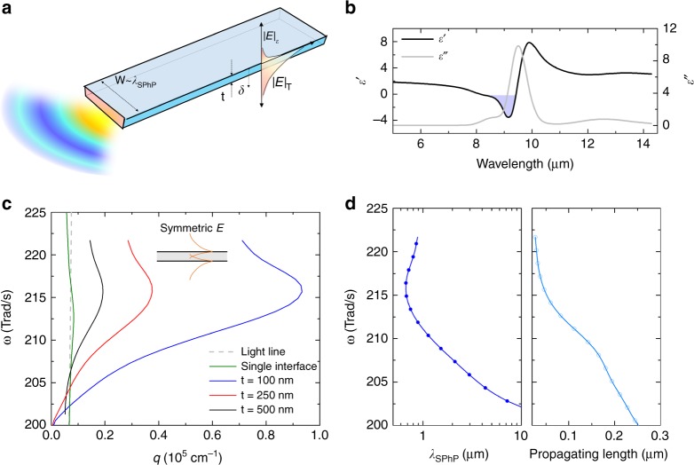
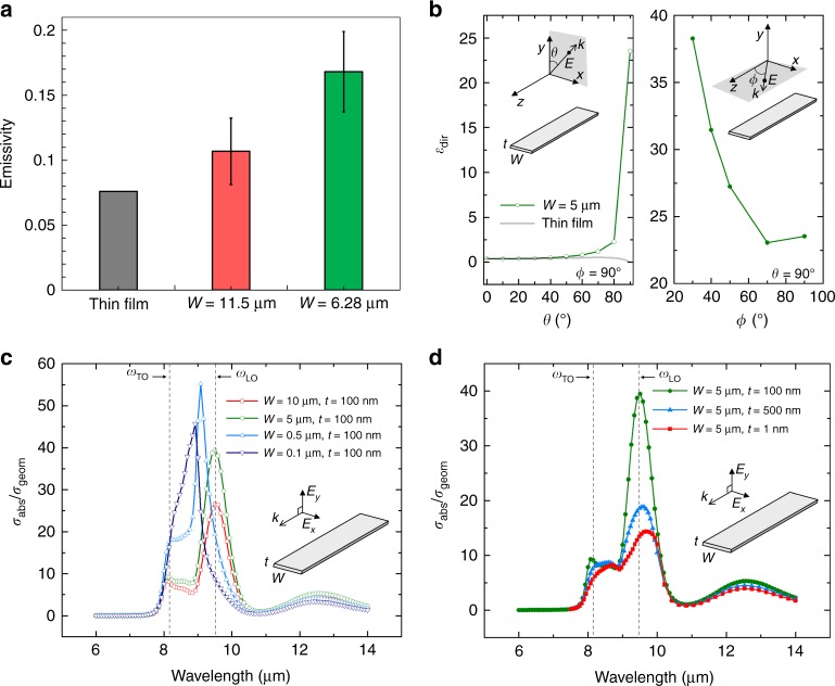
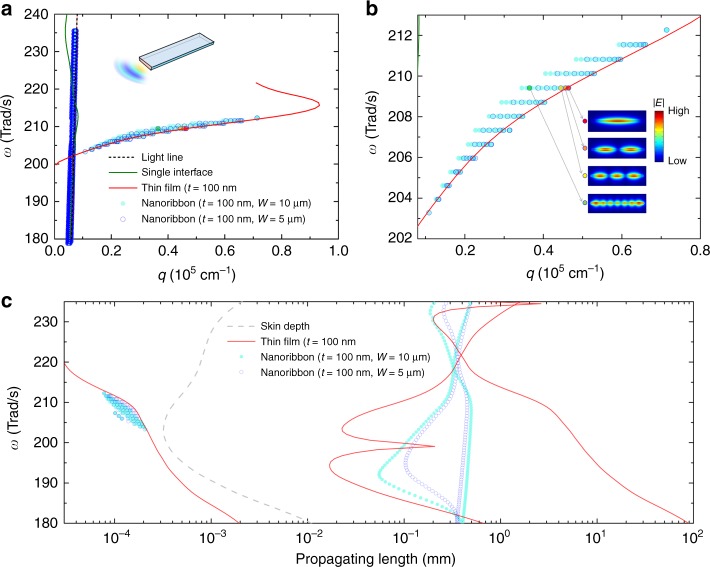
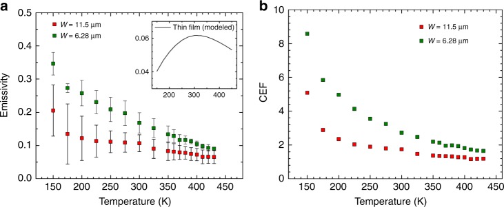
Coherent thermal emission deviates from the Planckian blackbody emission with a narrow spectrum and strong directionality. While far-field thermal emission from polaritonic resonance has shown the deviation through modelling and optical characterizations, an approach to achieve and directly measure dominant coherent thermal emission has not materialised. By exploiting the large disparity in the skin depth and wavelength of surface phonon polaritons, we design anisotropic SiO2 nanoribbons to enable independent control of the incoherent and coherent behaviours, which exhibit over 8.5-fold enhancement in the emissivity compared with the thin-film limit. Importantly, this enhancement is attributed to the coherent polaritonic resonant effect, hence, was found to be stronger at lower temperature. A thermometry platform is devised to extract, for the first time, the thermal emissivity from such dielectric nanoemitters with nanowatt-level emitting power. The result provides new insight into the realisation of spatial and spectral distribution control for far-field thermal emission.


Conflict of interest statement

The authors declare no competing interests.

Figures

Fig. 1
Fig. 1
Anisotropic nanoribbon for localised resonance by polaritons. a Schematic illustration of a long nanoribbon with rectangular cross-section with thickness (t) and width (W). Here, t is thinner than the skin depth (δ), leading to significant transmitted intensity of the electromagnetic wave perpendicular to the ribbon ET compared with the absorbed intensity Eε. Otherwise, the optical response in the parallel direction to the plane would yield higher emission because the cross-sectional length scale with the integer multiples of half wavelength supports the localised resonance modes, enhancing the absorption cross-section. b Plots of the real and imaginary permittivity of SiO2. The region of the Reststrahlen band is coloured. c Dispersion relation of SPhP supported by thin films of different thickness, calculated from the approximate solution Eq. (1). The energy range is within the Reststrahlen band. d SPhP wavelength and propagating length for a 100 nm thick thin film, corresponding to the dispersion curve
Fig. 2
Fig. 2
Suspended thermal transport measurement micro-device with monolithic SiO2 nanoribbon. a Schematic illustration and b SEM image of the device showing the suspended heater and sensor electrodes (Pt) and a monolithic SiO2 nanoribbon across the electrodes. cf SEM images of SiO2 nanoribbons of various sizes. All the scale bars represent 30 μm
Fig. 3
Fig. 3
Thermal transport measurement methodology and results. a Schematic illustration of heat-transfer process in the suspended micro-device with SiO2 nanoribbon overlaid with the colour code representing the temperature rise (θ) on the heater, sensor, and nanoribbon. The schematic plot at the bottom presents profiles of θ along the ribbon: when there is no heat loss (the fin parameter m = 0), the θ profile is a straight line (dashed line), and when there is radiative heat loss (m > 0), θ is exponentially decayed along the length (solid line). b AC modulated heating scheme. The heating beam is heated by a 1ω current, and the corresponding resistance change (ΔRh) due to the temperature rise is measured from the 3ω voltage. The sensing beam resistance change, ΔRs, was measured from the 2ω voltage using a small DC excitation current (Is,DC). A Wheatstone bridge configuration was used on the sensing side to increase the measurement sensitivity. c, d Plots of measured apparent thermal conductivity (kapp) vs. temperature for nanoribbon widths of 11.5 μm (c) and 6.28 μm (d). kapp was calculated using Eq. (6), which assumes a linear temperature profile along the ribbon (i.e., the dashed line in a with m = 0 or no radiation heat loss). The further below kapp is from the true thermal conductivity of SiO2, the larger the radiative heat loss. The error bars were determined by the standard deviations from the conductance measurement. e, f Plots of temperature ratios, Δ, between the heating and sensing beams as a function of temperature. Δ is defined as γ/γlossless and is a measure of the radiative heat loss. The experimental results (symbols) are compared to the fitted fin model (dotted lines), and the coloured area indicates the uncertainties of the fitted emissivity values
Fig. 4
Fig. 4
Enhanced emissivity with anisotropic nanoribbons. a Plots of the extracted emissivity at room temperature for ribbon widths of 6.28 and 11.5 μm, where the error bars are corresponding to the uncertainty in the fitting as shown in Fig. 3e, f. The grey bar represents the computed emissivity of an infinitely wide thin film of the same thickness as the ribbons, i.e., 100 nm. b Plots of directional emissivity (εdir) of a nanoribbon with W = 5 µm at a wavelength of 9.5 µm, where the incoming plane wave has propagation (k) directions where the polarisation directions are normal to k in xy plane and xz plane, respectively for each φ = 90° and θ = 90° cases, and its incident angle is controlled by θ and φ as shown in the insets. c, d Enhanced absorption cross-sectional area as a function of wavelength, where the absorption cross-sectional area (σabs) is normalised by the geometrical cross-section (σgeom) for various widths (c) and thicknesses (d)
Fig. 5
Fig. 5
Numerical mode analysis of nanoribbons. a Dispersions of nanoribbons by numerical modelling. The numerical results (symbols) were compared to the analytical results of light line, single interface and a thin film. b Zoomed-in plots of (a). The insets represent the electric field intensity distributions in the cross-section of a 5-µm wide nanoribbon at the four colour-filled symbols. c Propagating lengths of nanoribbons with 5 and 10 µm widths, corresponding to the dispersion in (a, b)
Fig. 6
Fig. 6
Temperature-dependent emissive behaviour. a Plots of emissivity as a function of temperature, where the error bars correspond to the uncertainty in the fitting as shown in Fig. 3e, f. The inset shows the modelled emissivity of an infinite thin film. b Plots of coherent enhancement factor (CER) as a function of temperature

References

    1. Planck, M. The Theory of Heat Radiation (Courier Corporation, P. Blakiston’s Son & Co., Philadelphia, 1914).
    1. Song B, et al. Radiative heat conductances between dielectric and metallic parallel plates with nanoscale gaps. Nat. Nanotechnol. 2016;11:509–514. doi: 10.1038/nnano.2016.17. - DOI - PubMed
    1. Narayanaswamy A, Shen S, Chen G. Near-field radiative heat transfer between a sphere and a substrate. Phys. Rev. B. 2008;78:115303. doi: 10.1103/PhysRevB.78.115303. - DOI
    1. Shen S, Narayanaswamy A, Chen G. Surface phonon polaritons mediated energy transfer between nanoscale gaps. Nano Lett. 2009;9:2909–2913. doi: 10.1021/nl901208v. - DOI - PubMed
    1. Cui LJ, et al. Study of radiative heat transfer in Ångström- and nanometre-sized gaps. Nat. Commun. 2017;8:14479. - PMC - PubMed

Publication types