Review
. 2019 Jan 11;6(6):1801445.
doi: 10.1002/advs.201801445. eCollection 2019 Mar 20.

Recent Progress in Inkjet-Printed Thin-Film Transistors

Affiliations
Review

Recent Progress in Inkjet-Printed Thin-Film Transistors

Seungjun Chung et al. Adv Sci (Weinh). .

Abstract

Drop-on-demand inkjet printing is one of the most attractive techniques from a manufacturing perspective due to the possibility of fabrication from a digital layout at ambient conditions, thus leading to great opportunities for the realization of low-cost and flexible thin-film devices. Over the past decades, a variety of inkjet-printed applications including thin-film transistors (TFTs), radio-frequency identification devices, sensors, and displays have been explored. In particular, many research groups have made great efforts to realize high-performance TFTs, for application as potential driving components of ubiquitous wearable electronics. Although there are still challenges to enable the commercialization of printed TFTs beyond laboratory-scale applications, the field of printed TFTs still attracts significant attention, with remarkable developments in soluble materials and printing methodology. Here, recent progress in printing-based TFTs is presented from materials to applications. Significant efforts to improve the electrical performance and device-yield of printed TFTs to match those of counterparts fabricated using conventional deposition or photolithography methods are highlighted. Moreover, emerging low-dimension printable semiconductors, including carbon nanotubes and transition metal dichalcogenides as well as mature semiconductors, and new-concept printed switching devices, are also discussed.

Keywords: flexible devices; inkjet printing; solution processes; switching devices; thin‐film transistors.


Conflict of interest statement

The authors declare no conflict of interest.

Figures

Figure 1
Figure 1
a) Functional electronic inks for realizing high‐performance inkjet‐printed TFTs. b) Scheme of sequential inkjet printing process on a flexible substrate.
Figure 2
Figure 2
Schemes of various printing techniques: a) inkjet printing, b) spray printing, c) gravure printing, d) flexographic printing, and e) screen printing.
Figure 3
Figure 3
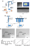
a) Inkjet printing system, captured image of an in‐flight ink droplet from (top) a single nozzle, (bottom) cartridge‐type nozzle, and example optical image of a printed TFT (G: gate, S and D: source and drain electrodes, C: channel). b) Schematic of droplet ejection in piezoelectric nozzles: (left) a single nozzle, (right) cartridge‐type nozzle. c) Top‐view optical images of the cartridge‐type nozzles having a diameter of 20 µm (left) and 10 µm (right). (The ejected droplets having a volume of ≈10 pL (left) and ≈1 pL (right) in flight are also included.) The droplet size and velocity from a 20 µm diameter nozzle depending on the maximum voltage of the input pulse train.
Figure 4
Figure 4
a) Jettable window within the capillary number–Weber number parameter space. The solvent systems used to create the window are oxylene, tetralin, anisole, decanol, hexanol, octanol, and binary solvent mixtures of hexanol/octanol, octanol/decanol, decanol/cyclohexanol, and oxylene/tetrahydrofuran. b) Drop stability breakdown mechanisms corresponding to the first four regions of the jettability window. c) Multiple droplet breakups resulting from wavelike instability corresponding to the stability breakdown in region IV. Reproduced with permission.72 Copyright 2014, American Chemical Society.
Figure 5
Figure 5
Fluid‐flow‐enhanced crystal growth. a) Schematic of solution shearing using a micropillar‐patterned blade. The arrow indicates the shearing direction. b) A scanning electron micrograph of a micropillar‐patterned blade. Inset: Top view of the micropillars under an optical microscope. The pillars are 35 µm wide and 42 µm high. c) Streamline representation of simulated fluid flow around the micropillars. The arrow indicates the flow direction. The streamlines are colour coded to indicate the scale of velocity (mm s−1), ranging from 0 (deep blue) to 1.3 mm s−1. d–f) Cross‐polarized optical micrograph of a TIPS‐pentacene film coated from its mesitylene solution with (d) (right), (f) and without micropillars (d) (left), (e) at a shearing speed of 0.6 mm s−1. Reproduced with permission.98 Copyright 2013, Springer Nature.
Figure 6
Figure 6
Inkjet printing of organic single‐crystal thin films. a) Schematic of the process. Antisolvent ink (A) is first inkjet‐printed (step 1), and then solution ink (B) is overprinted sequentially to form intermixed droplets confined to a predefined area (step 2). Semiconducting thin films grow at liquid–air interfaces of the droplet (step 3), before the solvent fully evaporates (step 4). b) Micrographs of a 2037 array of inkjet‐printed C8‐BTBT single‐crystal thin films. c) Crossed Nicols polarized micrographs of the film. d) Expanded micrograph of the film, showing stripes caused by molecular‐layer steps. e) Atomic force microscopy image and the height profile (below) showing the step‐and‐terrace structure on the film surfaces. Reproduced with permission.100 Copyright 2011, Springer Nature.
Figure 7
Figure 7
SWCNT solution shearing technique. a) Schematic depiction of SWCNT alignment using solution shearing. AFM phase image of sheared SWCNTs on b) 1.2 µm and c) 0.6 µm wide solvent‐wetting regions. The images show better alignment of SWCNTs on the 0.6 µm wide solvent‐wetting strips. The insets are height profiles obtained using topography images. Reproduced with permission.156 Copyright 2015, Wiley‐VCH.
Figure 8
Figure 8
Basic characterization of nanosheets and nanosheet networks. a) Photo of dispersions of MoS2, MoSe2,WS2, and WSe2 (C ≈ 0.2 mg mL−1). b) Typical TEM image of liquid‐exfoliated WSe2 nanosheets. c) Optical absorption spectra (extinction minus scattering) measured on nanosheet dispersions (C ≈ 0.005 mg mL−1). d) Plot of nanosheet length versus thickness (layer number N) for all materials. The horizontal line approximately separates thinner nanosheets with N‐dependent bandgap from thicker ones with bulk‐like bandgap. Inset: Typical AFM image. e) Typical scanning electron microscopy (SEM) images of a sprayed network of WSe2 nanosheets. f) Raman spectra measured on networks of all four materials. g) Measured network density plotted versus nanosheet density; the resultant porosity values P are indicated. Reproduced with permission.179 Copyright 2017, American Association for the Advancement of Science.
Figure 9
Figure 9
a) OM image of screen‐printed graphene for gate (G), source (S), and drain (D) electrodes on glassine paper. b) Photograph of a 3 × 4 array of organic TFTs. c,d) Representative transfer and output characteristics, respectively; the transfer curve was collected with a voltage sweep rate of 50 mV s−1. e–i) Histograms of device metrics for 40 devices (4 batches × 10 devices), including the on‐current (I on), off‐current (I off), on/off‐current ratio (I on/I off), charge carrier mobility (µ), and threshold voltage (V th), respectively. Reproduced with permission.198 Copyright 2015, Wiley‐VCH.
Figure 10
Figure 10
a) Optical and schematic images of an all‐inkjet‐printed inverter using two p‐type OTFTs. b) Schematic diagrams of the PS brush treatment procedure on the PVP gate dielectric and Ag S/D electrodes (20 nm thick PS‐Si(CH3)2Cl layers were inkjet‐printed to cover all the UV/O3‐treated Ag electrodes/PVP gate dielectrics. Subsequently, they were annealed at 110 °C for 1 h and then rinsed with an excess of toluene). c) XPS profiles for Si 2p and N 1s intensity of the bare and PS brush treated PVP gate dielectrics before and after rinsing with toluene. All‐inkjet‐printed p‐type OTFT d,e) transfer (V DS of −5 and −20 V under V GS multisweeps from 20 to −30 V) and f,g) output characteristics d,f) without and e,g) with a PS brush interlayer. Reproduced with permission.95 Copyright 2013, Wiley‐VCH.
Figure 11
Figure 11
a) 3D schematic cross‐section of the 3D‐complementary OFETs (3D‐COFET) with a bottom‐gate p‐type FET (PFET) vertically stacked on a top‐gate n‐type FET (NFET). b) Top view of 56 pairs of 3D‐COFET inverters fabricated by inkjet printing on a substrate. c) Microscope images of a 3D‐COFET inverter and d) printed active regions (white dotted areas) observed from the bottom (NFET) and the top (PFET) FETs by optical microscopy (scale bars = 200 µm). e) Transfer characteristics (|I DS| vs V GS) and f) output characteristics (|I DS| vs V DS with 2 V step V GS) of the NFET (red, left graphs) and the PFET (blue, right graphs). Reproduced with permission.207 Copyright 2016, American Chemical Society.
Figure 12
Figure 12
a) Micrographs of various printed digital circuits. b) Illustration of the piezoelecric pressure sensor and accelerometer fabrication. c) Printed temperature label with memory and Writing temperature dose signals into memory. Reproduced with permission.42 Copyright 2015, IEEE.
Figure 13
Figure 13
a) Schematic representation of the chemically controlled destabilization and flocculation process of the printed nanoink droplets. The NaCl loaded semiconducting oxide nanoinks show spontaneous stabilizer removal from the nanoparticle surface during the ink drying process. Stability of the In2O3 nanoinks with PAANa as the stabilizing ligands and different halide ion concentration. b) In2O3 nanoink with 20 × 10−3 m NaCl, after 2 months of ink preparation. c) In2O3 nanoink with 50 × 10−3 m NaCl, after 1 h of ink preparation. d) DLS particle size distribution of the In2O3 nanoink with 20 × 10−3 m NaCl concentration, as a function of the elapsed time. Surface morphology of the printed In2O3 thin films, SEM images showing surface topography of the printed droplets from nanoparticulate inks that contain e) no NaCl and f) 20 × 10−3 m NaCl, respectively. Reproduced with permission.132 Copyright 2015, American Chemical Society.
Figure 14
Figure 14
a) ACO inks plotted on a Capillary (Ca) number/Weber (We) number diagram with empirically determined jettable window shaded in green and Z numbers 10 and 100 indicated by dashed lines. b) Stroboscopic snapshots of ACO droplets jetted from the piezoelectric print head by the corresponding jetting waveform. c) Array of inkjet‐printed transparent conductive lines. d) Diagram of oxide TFT structure with printed semiconductor and printed S/D electrodes with matching optical micrograph. e) Height profile of InOx‐printed transistor measured transverse to ACO electrodes. f) Surface tension of aqueous inks formulated from aluminum, indium, and cadmium nitrate salts. g) Transfer characteristics with linear mobility shown and h) output characteristics of aqueous InOx‐printed transistor with printed ACO contacts processed at ≤250 °C. Reproduced with permission.133 Copyright 2017, Wiley‐VCH.
Figure 15
Figure 15
The morphology of isolated ZrO2 droplet patterns as a function of substrate temperature on PMMA‐coated substrates: a) surface profiles and b) typical cross‐sectional profiles. c) Cross‐sectional profile of the fabricated TFTs. The inset shows the fabricated TFTs. d) Surface profiles of the TFT fabricated on a glass substrate. The inset shows the optical image. Representative TFT characteristics: e) I dV d and f) I dV g (left axis) and I d 0.5V g (right axis). Reproduced with permission.221 Copyright 2015, Wiley‐VCH.
Figure 16
Figure 16
Fully printed and intrinsically stretchable carbon nanotube thin‐film transistors (TFTs) and integrated logic circuits. a) Schematic illustrating the structure of a printed stretchable TFT. Unsorted carbon nanotubes, high‐purity semiconducting single‐walled carbon nanotubes (SWCNT), and BaTiO3/PDMS composite are used as the source/drain/gate electrodes, channel semiconductor, and gate dielectric, respectively. b) Optical micrograph of a TFT printed on a PDMS substrate. c–e) Scanning electron micrograph of c) the carbon nanotube network in the source/drain electrodes and d) channel and e) atomic force micrograph of the BaTiO3/PDMS gate dielectric. f) Optical photograph of a representative sample consisting of four TFTs, a resistive load inverter, and a resistive load two‐input NOR gate and NAND gate, at tensile strains of 0% (top), ≈25% (middle), and ≈50% (bottom). Reproduced with permission.162 Copyright 2016, American Chemical Society.
Figure 17
Figure 17
All‐printed, all‐nanosheet TFT. a) Schematic showing all‐printed TFT structure. The source, drain, and gate electrodes are inkjet‐printed networks of graphene nanosheets; the channel is an inkjet‐printed network of WSe2 nanosheets. The gate electrode is separated from the channel by a spray‐cast BN nanosheet network. The entire porous volume of the structure is filled with an ionic liquid to facilitate electrolytic gating. b) Photographs of the printing steps. From left to right: Graphene source (s) and drain (d) electrode (t ≈ 400 nm); the WSe2 channel (t ≈ 1 mm, L = 200 mm, w = 16 mm); the BN separator (t ≈ 8 mm); and finally the graphene gate (g, t ≈ 400 nm). c) A flexible array of printed TFTs. d) Cross‐sectional SEM image showing WSe2 channel and BN separator. e) Magnified image of BN network showing porosity (P = 60%). f) Transfer curves for a printed TFT with a WSe2 active channel after cycling the gate voltage 1, 10, 25, and 50 times. Reproduced with permission.179 Copyright 2017, American Association for the Advancement of Science.
Figure 18
Figure 18
a) Schematic illustration of the fabrication processes for fully printed, flexible, and transparent CVD‐synthesized MoS2 phototransistors. b) I DSV GS curves using a log scale at V DS = 1 V. Inset represents the I DSV GS curves using a linear scale. The ratio of I light (= I ph + I dark) to I dark in the ON and OFF states as a function of c) wavelength and d) laser power at a fixed V DS = 10 V. Insets of (c) and (d) exhibit I ph versus V GS and the change in V th with respect to the laser power, respectively. As the laser power increased, V th shifted in the negative voltage direction, which indicates an increase in I ph in the subthreshold regime. Reproduced with permission.247 Copyright 2017, American Chemical Society.
Figure 19
Figure 19
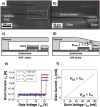
Printed MEM switch fabricated using nanoparticle ink. Scanning electron micrographs of a) multiple printed MEM switches and b) close‐up view of one switch. The source beam is anchored to the source pad; the two other electrodes (actuating gate and contacting drain) are located underneath the source beam. Schematic cross‐sectional illustration of the three‐terminal switch structure c) in the OFF‐state and d) in the ON‐state. Measured e) I DSV GS and f) I DSV DS characteristics of the printed MEM switch. Reproduced with permission.252 Copyright 2013, American Chemical Society.
Figure 20
Figure 20
SEM images of inkjet‐printed MEM reed relay. a) Drain reed blocks the curling of source reed, b) close‐up image of the drain and the source reed contact region, c) close‐up image of the suspended source reed showing the air gap. Switching characteristics of inkjet‐printed reed relays. I DSV GS characteristics of the reed relay with varying drain bias (V DS) for d) 5.5 µm and e) 4.5 µm thick source reed showing abrupt switching with turn‐off voltages (V TOF) of ≈15 and ≈11 V, respectively. These devices also show high on‐current and noise level off‐current that are in the noise floor of the parameter analyzer. Very low on resistances (R ON) of 12.88 and 14.26 Ω are extracted from the I DSV DS characteristics for f) 5.5 µm and g) 4.5 µm thick source reed, respectively. Reproduced with permission.255 Copyright 2015, Wiley‐VCH.
Figure 21
Figure 21
An artificial afferent nerve system in comparison with a biological one. a) A biological afferent nerve that is stimulated by pressure. Pressures applied onto mechanoreceptors change the receptor potential of each mechanoreceptor. The receptor potentials combine and initiate action potentials at the heminode. The nerve fiber forms synapses with interneurons in the spinal cord. Action potentials from multiple nerve fibers combine through synapses and contribute to information processing. b) An artificial afferent nerve made of pressure sensors, an organic ring oscillator, and a synaptic transistor. Only one ring oscillator connected to a synaptic transistor is shown here for simplicity. However, multiple ring oscillators with clusters of pressure sensors can be connected to one synaptic transistor. The parts with the same colors in (a) and (b) correspond to each other. c) A photograph of an artificial afferent nerve system. Reproduced with permission.261 Copyright 2018, American Association for the Advancement of Science.
Figure 22
Figure 22
Fully printed organic thin‐film transistors on ultraflexible films. a) A photograph of organic TFT devices on 1 mm thick parylene‐C films. The devices were fabricated entirely with printing processes. Scale bar, 2 cm. b) Cross‐sectional diagram of a thin organic TFT device. c) A polarization microscope image of the channel region. Scale bar, 100 mm. d) Top‐view photograph of a completed 10 cm × 10 cm fully printed 20 × 20 TFT array fabricated on an ultraflexible parylene‐C film. Scale bar, 1 cm. e) A magnified view of six TFT devices. Scale bar 2 mm. f) Flexible TFT array sheet conforming to a human throat. Reproduced with permission.196 Copyright 2014, Springer Nature.

References

    1. Gao W., Emaminejad S., Yin Nyein H. Y., Challa S., Chen K., Peck A., Fahad H. M., Ota H., Shiraki H., Kiriya D., Lien D.‐H., Brooks G. A., Davis R. W., Javey A., Nature 2016, 529, 509. - PMC - PubMed
    1. Imani S., Bandodkar A. J., Mohan A. M. V., Kumar R., Yu S., Wang J., Mercier P. P., Nat. Commun. 2016, 7, 11650. - PMC - PubMed
    1. Koh A., Kang D., Xue Y., Lee S., Pielak R. M., Kim J., Hwang T., Min S., Banks A., Bastien P., Manco M. C., Wang L., Ammann K. R., Jang K. I., Won P., Han S., Ghaffari R., Paik U., Slepian M. J., Balooch G., Huang Y., Rogers J. A., Sci. Transl. Med. 2016, 8, 366ra165. - PMC - PubMed
    1. Drotlef D.‐M., Amjadi M., Yunusa M., Sitti M., Adv. Mater. 2017, 29, 1701353. - PubMed
    1. Han S., Kim M. K., Wang B., Wie D. S., Wang S., Lee C. H., Adv. Mater. 2016, 28, 10257. - PubMed

LinkOut - more resources