

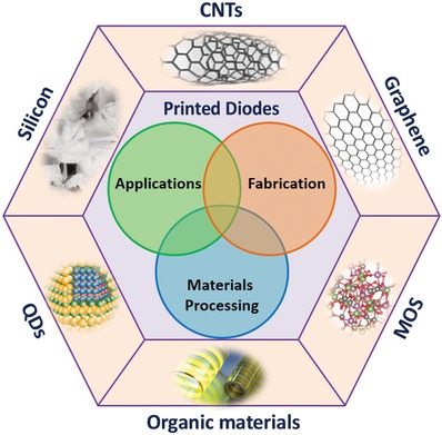
Printed Diodes: Materials Processing, Fabrication, and Applications
- PMID: 30937260
- PMCID: PMC6425440
- DOI: 10.1002/advs.201801653
Printed Diodes: Materials Processing, Fabrication, and Applications
Abstract
Printing techniques for the fabrication of diodes have received increasing attention over the last decade due to their great potential as alternatives for high-throughput and cost-effective manufacturing approaches compatible with both flexible and rigid substrates. Here, the progress achieved and the challenges faced in the fabrication of printed diodes are discussed and highlighted, with a focus on the materials of significance (silicon, metal oxides, nanomaterials, and organics), the techniques utilized for ink deposition (gravure printing, screen printing, inkjet printing, aerosol jet printing, etc.), and the process through which the printed layers of diode are sintered after printing. Special attention is also given to the device applications within which the printed diodes have been successfully incorporated, particularly in the fields of rectification, light emission, energy harvesting, and displays. Considering the unmatched production scalability of printed diodes and their intrinsic suitability for flexible and wearable applications, significant improvement in performance and intensive research in development and applications of the printed diodes will continuously progress in the future.
Keywords: nanomaterials; organic light‐emitting diodes (OLEDs); printed diodes; printing technologies; radio frequency identifications (RFIDs).
Conflict of interest statement
The authors declare no conflict of interest.
Figures


References
-
- Semple J., Georgiadou D. G., Wyatt‐Moon G., Gelinck G., Anthopoulos T. D., Semicond. Sci. Technol. 2009, 206, 588.
-
- Wong W. S., Salleo A., Flexible Electronics: Materials and Applications, Vol. 11, Springer Science & Business Media, New York, USA: 2009.
-
- Berggren M., Nilsson D., Robinson N. D., Nat. Mater. 2007, 6, 3. - PubMed
-
- a) Rost H., Mildner W., Kunstst. Int. 2008, 98, 60;
- b) Sengupta D. L., Sarkar T. K., Sen D., Proc. IEEE 1998, 86, 235.
-
- Brütting W., Physics of Organic Semiconductors, WILEY‐VCH Verlag GmbH & Co. KGaA, Weinheim, Germany: 2006.
Publication types
Grants and funding
LinkOut - more resources
Full Text Sources
Other Literature Sources