. 2019 Apr 5;10(1):1574.
doi: 10.1038/s41467-019-09079-z.

Origin of apparent light-enhanced and negative capacitance in perovskite solar cells

Affiliations

Origin of apparent light-enhanced and negative capacitance in perovskite solar cells

Firouzeh Ebadi et al. Nat Commun. .

Abstract

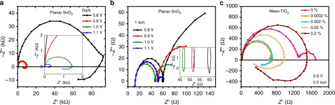
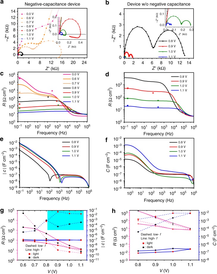
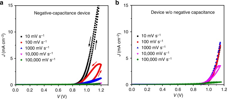
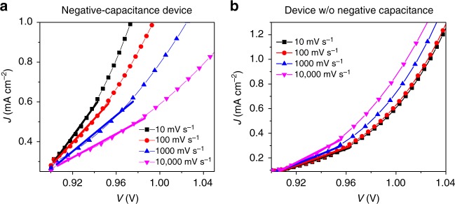
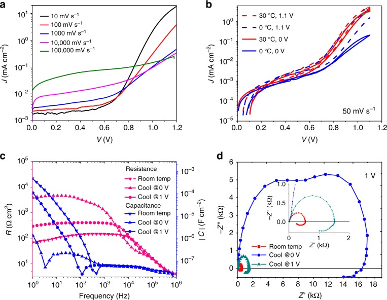
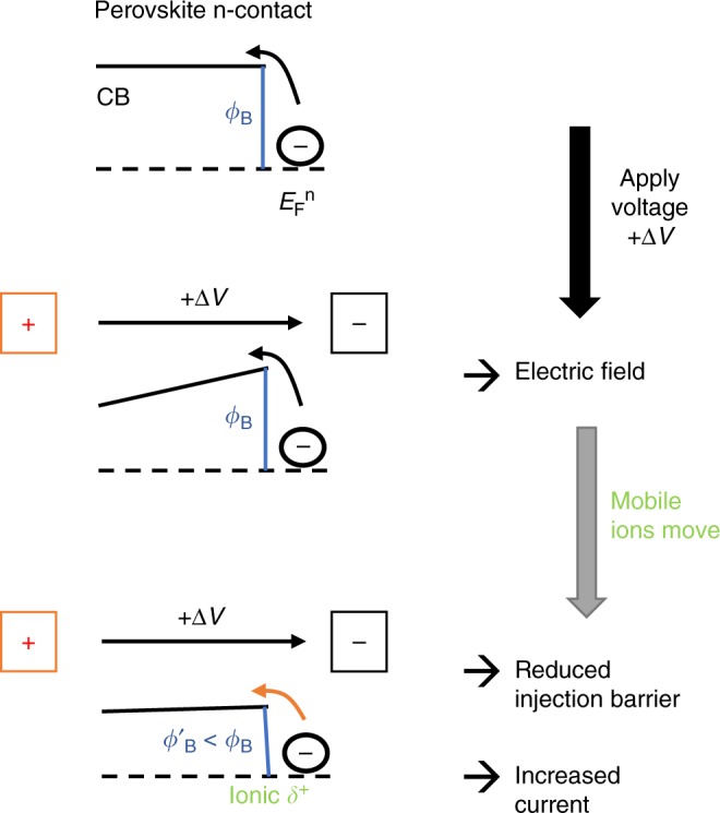
So-called negative capacitance seems to remain an obscure feature in the analysis of the frequency-dependent impedance of perovskite solar cells. It belongs to one of the puzzling peculiarities arising from the mixed ionic-electronic conductivity of this class of semiconductor. Here we show that apparently high capacitances in general (positive and negative) are not related to any capacitive feature in the sense of a corresponding charge accumulation. Instead, they are a natural consequence of slow transients mainly in forward current of the diode upon ion displacement when changing voltage. The transient current leads to a positive or negative 'capacitance' dependent on the sign of its gradient. The 'capacitance' appears so large because the associated resistance, when thinking of a resistor-capacitor element, results from another physical process, namely modified electronic charge injection and transport. Observable for a variety of devices, it is a rather universal phenomenon related to the hysteresis in the current-voltage curve.


Conflict of interest statement

The authors declare no competing interests.

Figures

Fig. 1
Fig. 1
Nyquist plots for different perovskite solar cells, operated under forward bias. The frequency range is from 1 MHz to 0.1 Hz. a, b Planar device based on SnO2 at different voltages, where negative capacitance can be observed in the dark a and a loop feature under light b. c Mesoporous TiO2-based devices with more pronounced negative capacitance for higher bismuth content in the perovskite (in the legend given as at.% referred to Pb)
Fig. 2
Fig. 2
EIS data as a function of applied voltage in the dark. Left: negative-capacitance device (0.02% Bi). Right: device without negative capacitance (0% Bi). a, b Nyquist plots showing approximately two semi-circles and the appearance of negative capacitance for voltages larger than 0.7 V. c, d Real part of impedance, visualizing the electrode series resistance for frequencies >105 Hz, a plateau at 1 kHz, and a higher (lower for negative C) low-f resistance. The symbols indicate the differential resistance obtained from JV scans with 10 mV s−1 (circles) and 10 V s−1 (stars). e, f Apparent capacitance Im(1Z)ω, where in e C values for frequencies lower than the one where the dip occurs are negative. g, h Resistance and capacitance (negative values shaded) obtained by describing the EIS data measured in the dark and under 1 sun by two RC elements in series. Rlow f ∝ 1/Clow f is striking, in particular in h
Fig. 3
Fig. 3
Time constants extracted from EIS data for different light intensities. a Negative-capacitance device. The capacitance changes sign at 0.8 V and the shaded area describes negative values, where the impedance data were fitted with multiple time constants. Details in Supplementary Table 1. b Device without negative capacitance. In both cases, the τlow f remains independent of voltage and illumination at around 0.1 s. The data were extracted from the EIS data shown in Fig. 2
Fig. 4
Fig. 4
Transient current response upon applying a voltage step in the dark. a Negative-capacitance device at 0.9 V after applying +20 mV at time 0. Apart from fast capacitive responses, a transient increase of the current is observed that is the origin of the apparent negative capacitance. b Voltage dependence of the transients of a negative capacitance device. c Comparison of devices with differently pronounced negative capacitance
Fig. 5
Fig. 5
JV curves in the dark starting at 0 V for different scan rates. a Negative-capacitance device, b Device without negative capacitance. In case of negative capacitance, the dependence of forward current on scan rate is much more pronounced at lower scan rates
Fig. 6
Fig. 6
JV curves in the dark for different scan rates after equilibration at 0.9 V. a Negative-capacitance device, b Device without negative capacitance. The differential resistance is indicated by the lines. The trends in the resistance with scan rate are opposite between the two devices
Fig. 7
Fig. 7
JV curves for negative-capacitance device. a Logarithmic representation of the forward scan (0–1.2 V) of Fig. 5a, indicating an increased series resistance for faster scans. b JV curves (50 mV s−1) measured after equilibration at 0 V (solid) and 1.1 V (dashed), at 30 °C (red) and 0 °C (blue), showing a higher series resistance for lower temperatures. c and d EIS data obtained at different temperatures (cool means 0 °C). Cooling-down has been done while keeping the device either at 0 or 1 V to freeze different ion distributions. Cooling down at 0 V induces a higher resistance consistent with the JV data
Fig. 8
Fig. 8
Sketch explaining ion-enhanced charge-carrier injection at the contact. Here the n-side is shown. An analogous picture can be drawn for the p-side. Ion redistribution upon increasing the voltage by ΔV changes the injection barrier ϕB. More positive net ionic charge leads to a surface dipole that decreases ϕB. This effect enhances the current, which appears as a negative capacitance

References

    1. Kern R, Sastrawan R, Ferber J, Stangl R, Luther J. Modeling and interpretation of electrical impedance spectra of dye solar cells operated under open-circuit conditions. Electrochim. Acta. 2002;47:4213–4225. doi: 10.1016/S0013-4686(02)00444-9. - DOI
    1. Fabregat-Santiago F, et al. Correlation between photovoltaic performance and impedance spectroscopy of dye-sensitized solar cells based on ionic liquids. J. Phys. Chem. C. 2007;111:6550–6560. doi: 10.1021/jp066178a. - DOI
    1. Bisquert J, Garcia-Belmonte G, Pitarch Aacute, Bolink HJ. Negative capacitance caused by electron injection through interfacial states in organic light-emitting diodes. Chem. Phys. Lett. 2006;422:184–191. doi: 10.1016/j.cplett.2006.02.060. - DOI
    1. Ehrenfreund E, Lungenschmied C, Dennler G, Neugebauer H, Sariciftci NS. Negative capacitance in organic semiconductor devices: bipolar injection and charge recombination mechanism. Appl. Phys. Lett. 2007;91:012112. doi: 10.1063/1.2752024. - DOI
    1. Mora-Seró I, et al. Implications of the negative capacitance observed at forward bias in nanocomposite and polycrystalline solar cells. Nano Lett. 2006;6:640–650. doi: 10.1021/nl052295q. - DOI - PubMed

Publication types