Review
. 2017 Apr 23;9(4):150.
doi: 10.3390/polym9040150.

Electrical and Electrochemical Properties of Conducting Polymers

Affiliations
Review

Electrical and Electrochemical Properties of Conducting Polymers

Thanh-Hai Le et al. Polymers (Basel). .

Abstract

Conducting polymers (CPs) have received much attention in both fundamental and practical studies because they have electrical and electrochemical properties similar to those of both traditional semiconductors and metals. CPs possess excellent characteristics such as mild synthesis and processing conditions, chemical and structural diversity, tunable conductivity, and structural flexibility. Advances in nanotechnology have allowed the fabrication of versatile CP nanomaterials with improved performance for various applications including electronics, optoelectronics, sensors, and energy devices. The aim of this review is to explore the conductivity mechanisms and electrical and electrochemical properties of CPs and to discuss the factors that significantly affect these properties. The size and morphology of the materials are also discussed as key parameters that affect their major properties. Finally, the latest trends in research on electrochemical capacitors and sensors are introduced through an in-depth discussion of the most remarkable studies reported since 2003.

Keywords: conducting polymers; conductivity; electrochemistry; electronic properties; pseudocapacitors; sensors.


Conflict of interest statement

The authors declare no conflict of interest.

Figures

Figure 1
Figure 1
The structure of polyacetylene: The backbone contains conjugated double bonds.
Figure 2
Figure 2
The electronic band and chemical structures of polythiophene (PT) with (a) p-type doping and (b) n-type doping.
Figure 3
Figure 3
Electronic bands and chemical structures illustrating (a) undoped; (b) polaron; (c) bipolaron; and (d) fully doped states of polypyrrole (PPy).
Figure 4
Figure 4
(a) Schematic illustration of the geometric structure of a neutral soliton on a trans-polyacetylene chain; (b) A soliton band with light doping (left) and heavy doping (right); The band structure of trans-polyacetylene containing (c) a positively charged soliton; (d) a neutral soliton; and (e) a negatively charged soliton.
Figure 5
Figure 5
The general conductivity range of conducting polymers (CPs).
Figure 6
Figure 6
Cyclic voltammograms of a poly(N-phenyl-1-naphthylamine) film on Pt in 1 M LiClO4/CH3CN solution at different scanning rates. Reprinted with permission from [85]. Copyright 1990, American Chemical Society.
Figure 7
Figure 7
Cyclic voltammetry (CV) curves of a polyaniline (PANI) film doped with hydrochloric acid or sulfuric acid at the same potential scan rate 50 mV·s−1.
Figure 8
Figure 8
CV analysis of PANI nanostructures with three different shapes (nanosphere, NS; nanorods, NR; and nanofibers, NF) performed in a 1 M sulfuric acid solution. (a) Cyclic voltammograms of electrodes consisting of PANI nanostructures at the same scan rate (25 mV·s−1); (b) plots of the peak current (the anodic peak current, Ipa; the cathodic peak current, Ipc) vs. the scan rate; and (c) plots of the peak potential (the anodic peak potential, Epa; the cathodic peak current, Epc) vs. the log of the scan rate. With permission from [86]; Copyright 2012, American Chemical Society.
Figure 9
Figure 9
Mechanism of electrochemo-mechanical actuation in CPs. (a, c, e) Volume changes in CP via (b, d) two different redox pathways.
Figure 10
Figure 10
The different redox/protonation states and colors of PANI.
Figure 11
Figure 11
Field-emission scanning electron microscope images of PANI nanostructures with different aspect ratios synthesized under the same stirring conditions (200 rpm) and histograms showing their size distribution (D, diameter; L, length): (a) nanospheres; (b) nanorods; and (c) nanofibers. With permission from [86]; Copyright 2012, American Chemical Society.
Figure 12
Figure 12
Effect of binary nanoparticle packing on electrode performance. Ternary diagrams for nanospheres of three different diameters showing the distribution of (a,b) specific capacitance and (c,d) coulombic efficiency as a function of the mixed weight fraction (fm) measured at (a,c) 0.1 A·g−1 and (b,d) 1.0 A·g−1. A three-electrode system was used with 1 M sulfuric acid solution. The Ec values were calculated from the charge/discharge curves. Reprinted with permission from [123]. Copyright 2016, Royal Society of Chemistry.
Figure 13
Figure 13
(a) Schematic illustration of the formation of graphene/PANI multilayered nanostructures (GPMNs) by direct physical exfoliation of graphite with PANI glue; (b) photographs showing the long-term colloidal stability of a GPMN dispersion solution in the absence (left) and presence (right) of PANI glue. GPMNs showed outstanding colloidal stability in both NMP and water. Reprinted with permission from [126]. Copyright 2015, John Wiley & Sons.
Figure 14
Figure 14
Schematic of the synthetic procedure for NiCo2O4@PANI nanorod arrays. Reprinted with permission from [134]. Copyright 2016, American Chemical Society.
Figure 15
Figure 15
Real-time response of PPy/cellulose (PPCL) composite membranes in a flow cell measured at different applied potentials: (a) Hg(II); (b) Ag(I); (c) Pb(II); (d) Ni(II); (e) Cd(II); (f) Cr(III); and (g) Zn(II). Reprinted with permission from [152]. Copyright 2014, Royal Society of Chemistry.
Figure 16
Figure 16
Schematic illustrating (a) the alternating layered structure of graphene/PANI; (b) the series connection and parallel connection-like structures formed by different orientations of the graphene/PANI film between the electrodes; and (c,d) the resistometric sensor setup for measuring the electrical response of the graphene/PANI films (electrode, blue; PANI, green; graphene, black). Reprinted with permission from [153]. Copyright 2016, American Chemical Society.
Figure 17
Figure 17
Schematic illustration of the reaction steps for the fabrication of a field-effect transistor (FET) sensor platform based on carboxylated PPy nanotubes (CPNTs): (a) microelectrode substrate; (b) aminosilane-treated substrate; (c) immobilization of the nanotubes onto a substrate; and (d) binding of GOx to the nanotubes. Reprinted with permission from [154]. Copyright 2008, American Chemical Society.

References

    1. Hall N. Twenty-five years of conducting polymers. Chem. Commun. 2003;7:1–4. - PubMed
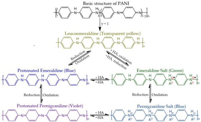
    1. Huang W.S., Humphrey B.D., MacDiarmid A.G. Polyaniline, a novel conducting polymer. Morphology and chemistry of its oxidation and reduction in aqueous electrolytes. J. Chem. Soc. Faraday Trans. 1. 1986;82:2385–2400. doi: 10.1039/f19868202385. - DOI
    1. McCullough R.D., Lowe R.D., Jayaraman M., Anderson D.L. Design, synthesis, and control of conducting polymer architectures: Structurally homogeneous poly(3-alkylthiophenes) J. Org. Chem. 1993;58:904–912. doi: 10.1021/jo00056a024. - DOI
    1. Wang J., Dai J., Yarlagadda T. Carbon nanotube conducting polymer composite nanowires. Langmuir. 2005;21:9–12. doi: 10.1021/la0475977. - DOI - PubMed
    1. Lee B.H., Lee J.H., Kahng Y.H., Kim N., Kim Y.J., Lee J., Lee T., Lee K. Graphene-conducting polymer hybrid transparent electrodes for efficient organic optoelectronic devices. Adv. Funct. Mater. 2014;24:1847–1856. doi: 10.1002/adfm.201302928. - DOI

LinkOut - more resources