Review
. 2019 Apr 17;9(2):57.
doi: 10.3390/bios9020057.

A Review on Surface-Enhanced Raman Scattering

Affiliations
Review

A Review on Surface-Enhanced Raman Scattering

Roberto Pilot et al. Biosensors (Basel). .

Abstract

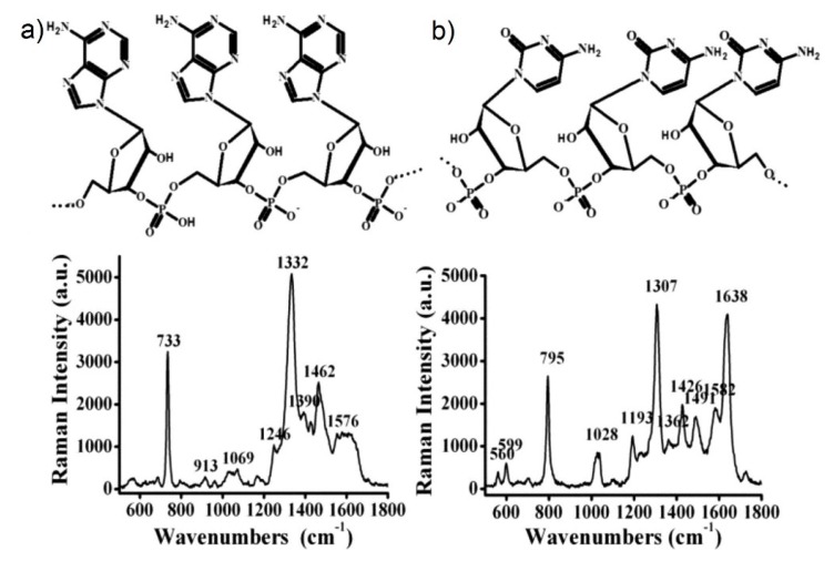
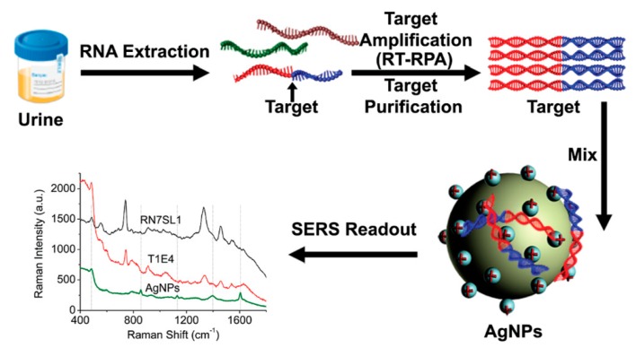
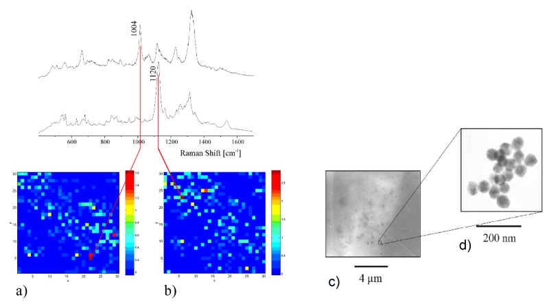
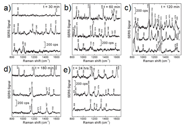
Surface-enhanced Raman scattering (SERS) has become a powerful tool in chemical, material and life sciences, owing to its intrinsic features (i.e., fingerprint recognition capabilities and high sensitivity) and to the technological advancements that have lowered the cost of the instruments and improved their sensitivity and user-friendliness. We provide an overview of the most significant aspects of SERS. First, the phenomena at the basis of the SERS amplification are described. Then, the measurement of the enhancement and the key factors that determine it (the materials, the hot spots, and the analyte-surface distance) are discussed. A section is dedicated to the analysis of the relevant factors for the choice of the excitation wavelength in a SERS experiment. Several types of substrates and fabrication methods are illustrated, along with some examples of the coupling of SERS with separation and capturing techniques. Finally, a representative selection of applications in the biomedical field, with direct and indirect protocols, is provided. We intentionally avoided using a highly technical language and, whenever possible, intuitive explanations of the involved phenomena are provided, in order to make this review suitable to scientists with different degrees of specialization in this field.

Keywords: Raman; SERS; biomedical applications; chemical enhancement; electromagnetic enhancement; enhancement factor; excitation wavelength; substrates; surface enhanced; underpotential deposition.


Conflict of interest statement

The authors declare no conflicts of interest.

Figures

Figure 1
Figure 1
Electromagnetic enhancement. (a) Normal Raman. A laser radiation, with electric field E(ωL) oscillating at (angular) frequency ωL impinges on a molecule, characterized by a Raman polarizability tensor α^R(ωR,ωL). The laser induces a dipole oscillating at the Raman frequency (vertical red arrow, p(ωR)); the Raman power radiated by this dipole is proportional to the square modulus of the dipole itself. (b) Surface enhanced Raman scattering (SERS) electromagnetic enhancement. When the molecule is placed near a plasmonic substrate, the electric field experienced by the molecule is ELoc(ωL), normally much stronger than the input laser E(ωL); this local field enhancement is quantified by MLocZ(ωL). Moreover, the presence of the plasmonic substrate also enhances the efficiency with which the dipole emits Raman radiation; this re-radiation enhancement is quantified by MLocZ(ωR). The total electromagnetic enhancement factor, within the |E|4 approximation, is defined as: GSERSEm=MLocZ(ωL)MLocZ(ωR). Chemical enhancement. (c) Normal Raman. The vibrational modes of a molecule in free space are characterized by the cross-section(s) σkfree; (d) SERS chemical enhancement. The interaction with the plasmonic substrate modifies the structure of the molecule and consequently also the cross-section(s) of its modes (σkads). The chemical enhancement is quantified as GSERSChem=σkadsσkfree.
Figure 2
Figure 2
MLocZ (MLoc in the figure) and MRad as a function of the wavelength are shown in panel (a,b), respectively. The molecule is placed 1 nm away from the surface of the silver nanoparticle (25 nm radius), along the direction in which the excitation laser is polarized (Z). Concerning the re-emission enhancement, MRad is the power emitted by the dipole integrated over the whole solid angle of emission; the molecular dipole can be oriented either parallel () or perpendicular () to the surface. Reproduced with permission from Le Ru et al. [6]. Copyright (2009), Elsevier B.V.
Figure 3
Figure 3
The molecule to metal and the metal to molecule charge transfer are illustrated in panels (a,b), respectively. |I, |K, and |F represent the molecular ground state, the molecular excited state(s), and the Fermi state of the metal, respectively. μKI, μIF, and μFK are the transition dipole moments. hFK and hIF are the Herzberg–Teller coupling parameters. Reprinted (adapted) with permission from Lombardi et al. [9]. Copyright (2008) American Chemical Society.
Figure 4
Figure 4
(a) Energy diagram for pyridine. The highest occupied molecular orbital (HOMO) energy has been approximated as the ionization energy of pyridine, determined from photoelectron spectroscopy measurements [142]; the energy difference between the lowest unoccupied molecular orbital (LUMO) and the Fermi level has been estimated with inverse photoemission spectroscopy [11]; the Fermi level of silver has been estimated by a photoelectric method [9,137,143]. (b) Energy diagram for the crystal violet cation. The HOMO and LUMO energies have been estimated with electrochemical methods [146].
Figure 5
Figure 5
(a) Spectral distribution of the plasmonic (red line), charge transfer (CT, black line), and intramolecular (green, blue, and violet lines) resonances for pyridine adsorbed on silver. Reprinted (adapted) with permission from Lombardi et al. [9]. Copyright (2008) American Chemical Society. (b) SERS spectrum of pyridine on silver. Reprinted (adapted) with permission from Lombardi et al. [137]. Copyright (2008), American Chemical Society.
Figure 6
Figure 6
Spectral distribution of the plasmonic (red line), CT (black line), and intramolecular (blue line) resonances for CV+ adsorbed on silver. Reprinted (adapted) with permission from Lombardi et al. [9]. Copyright (2008) American Chemical Society.
Figure 7
Figure 7
Collective oscillations of electrons in a spherical nanoparticle under the action of the external electric field.
Figure 8
Figure 8
Scattering, absorption, extinction, and local field efficiencies (QSCA(ω), QABS(ω), QE(ω), QNF(ω), respectively) for a silver nanoparticle with radius a = 22 nm immersed in water. These quantities are proportional to the corresponding cross-sections (i.e., QSCA(ω)=σSca(ω)πa2 and similarly for the others). Reproduced with permission from Messinger et al. [158]. Copyright (1981), American Physical Society.
Figure 9
Figure 9
The real and imaginary part of the dielectric constant are reported in panel (a,b), respectively. The data for gold, silver, and copper are taken from Johnson et al. [162]; the data for aluminum are taken from Palik [163]. Reproduced with permission from Pilot et al. [81]. Copyright (2018), Springer International Publishing AG.
Figure 10
Figure 10
Non-plasmonic electromagnetic enhancement in dielectric nanoparticles. (a) A dielectric sphere acts as a microlens, focusing light; (b) in a core-shell dielectric resonator, light is partially trapped inside the core. The Raman signal is amplified by the evanescent waves generated at the surface of the core. Reproduced with permission from Bontempi et al. [205]. Copyright (2018), John Wiley and Sons.
Figure 11
Figure 11
A dimer formed by two nanoparticles, separated by a gap g, is polarized by the action of an external electric field E0; a molecule is placed in the middle of the gap. E0 can be polarized along the main axis of the dimer (panel (a)) or perpendicularly to the axis (panel (b)). The blue arrows inside the nanoparticles represent the induced dipoles. This figure is inspired from Moskovits [221].
Figure 12
Figure 12
(a) The dimer under investigation is formed by two gold nanoparticles with radius a and separated by a gap g; the laser is polarized along the main axis. (b) Extinction coefficient for a single sphere and for the dimer (with different gaps) as a function of the wavelength. (c) Continuous lines: SERS enhancement (SERS EF in the figure) for a single sphere and for the dimer (with different gaps) as a function of the wavelength; the enhancement is calculated at the point where the surface of one of the two nanoparticles crosses the axis Z. Dashed line: SERS enhancement for the dimer with g = 2 nm, averaged over the whole metallic surface. Reproduced with permission from Le Ru et al. [6]. Copyright (2009) Elsevier B.V.
Figure 13
Figure 13
(a) GSERS distribution inside the 2 nm gap formed by two gold nanoparticles with a radius of 30 nm. The enhancement is calculated at the wavelength at which it reaches its maximum value. (b) Variation of GSERS along the (curved) surface of the nanoparticle (thin black line); the thick black line is not commented in this paper. Reproduced with permission from Etchegoin et al. [16].
Figure 14
Figure 14
The metallic substrate is represented by the hemispheroid; on top of it, the arachidic acid layer (spacer) and the phthalocyanine (Raman probe). Reproduced with permission from Kovacs et al. [235]. Copyright (1986), American Chemical Society.
Figure 15
Figure 15
SERS signal as a function of the distance from the surface. A short and a long-range component are identified; they are associated to morphological features of the metallic substrate with a size of approximately 1 nm and 20 nm, respectively. In the insets, a scanning electron microscopy (SEM) picture of the SERS substrate (silver film over nanospheres) and a simulation of the electric field are presented. Reproduced with permission from Masango et al. [236]. Copyright (2016), American Chemical Society.
Figure 16
Figure 16
(a). Absorption (dash red line), scattering (dash-dot green line), and extinction (solid black line) of human skin as a function of the wavelength. The three transparency windows are indicated as NIR-I, NIR-II, NIR-III. Reproduced with permission from Hemmer et al. [276]. Copyright (2013), the Royal Society of Chemistry. (b) Extinction coefficient of oxygenated blood (solid red line), deoxygenated blood (dotted blue line), skin (ochre dash line), and fatty tissues (green dash line). Reproduced with permission from Smith et al. [277]. Copyright (2009), Macmillan Publishers Limited.
Figure 17
Figure 17
Scattering intensity (red line) and enhancement factor (blue points) measured for the single gold nanoparticle dimer embedded in a silica shell shown in the inset. Reproduced with permission from Kleinman et al. [26]. Copyright (2013), American Chemical Society.
Figure 18
Figure 18
(a) SEM image of the SERS substrate fabricated by nanosphere lithography; (b) Extinction (blue line) and local field (dots and corresponding fit) distribution. Reproduced with permission from Michieli et al. [127] under Creative Commons 3.0 license (https://creativecommons.org/licenses/by/3.0/).
Figure 19
Figure 19
Example of reflectivity for an 1800 groove/mm grating optimized for use between 450 and 850 nm. Transverse electric (TE) indicate that the electric field of the radiation is polarized perpendicular to the plane of incidence; transverse magnetic (TM) indicate that the magnetic field of the radiation is polarized perpendicular to the plane of incidence; unpolarized is the average of TE and TM. Adapted with permission from Adar et al. [299].
Figure 20
Figure 20
Typical quantum efficiency of a silicon (black line) and of an Indium gallium arsenide (InGaAs, red line) detector: The first corresponds to a Symphony II front illuminated charged coupled device (CCD) and the second one to a Symphony II 1700 InGaAs linear array. Data adapted with permission from Horiba Scientific (https://www.horiba.com).
Figure 21
Figure 21
The reproducibility/uniformity and the Raman enhancement for a large number of substrates (Y axis) is correlated to the degree of order (X axis). The reproducibility/uniformity (short dashed line) increases with the degree or order of the substrate, while the enhancement (long dashed line) follows the opposite trend. For relevant applications, SERS substrates have to satisfy a tradeoff between the former and the latter. Reproduced with permission from Milton et al. [303]. Copyright (2008), John Wiley and Sons.
Figure 22
Figure 22
(a) Indirect protocol. A SERS tag is functionalized with antibodies and selectively binds to the analyte; its detection is carried out through the spectrum of the Raman reporter contained in the SERS tag. (b) Direct protocol. The analyte is adsorbed on the nanoparticle and detected through its own Raman spectrum. Reproduced with permission from Bonifacio et al. [304]. Copyright (2015), Springer-Verlag Berlin Heidelberg.
Figure 23
Figure 23
(a) Cyclic voltammetry in H2O + 5 mM CuSO4 + 0.1 M LiClO4 at glassy carbon, scan rate 0.2 V·s−1; (b) double potential pulse for the Cu deposition applied in this study. Adapted with permission from Durante et al. [254]. Copyright (2014), John Wiley and Sons.
Figure 24
Figure 24
(a) Dipstick/swab paper substrate: The SERS active region is printed in the top vertex; the inset is a SEM image showing the silver nanoparticles at the surface of cellulose fibers. (b) Substrate used as a swab to collect the analyte. (c) The swab/dipstick impregnated with the analyte is immersed in a solvent. The solvent flows through the paper substrate, wicked by capillary forces, and concentrates the analyte in the SERS active region. (d) Instrument used for collecting SERS spectra. Reproduced with permission from Yu et al. [393]. Copyright (2013), the Royal Society of Chemistry.
Figure 25
Figure 25
Illustration of the screen-printing process. The nanoparticle ink (a) and a screen plate (b) are used to print an array of SERS active areas with the help of a squeegee (c); SERS measurements are carried out on the printed spots (d). Reproduced with permission from Wu et al. [338] under Creative Commons 4.0 license (https://creativecommons.org/licenses/by/4.0/).
Figure 26
Figure 26
Illustration of the electrospinning process. Reproduced with permission from Greiner et al. [394]. Copyright (2007), John Wiley and Sons.
Figure 27
Figure 27
(a) Reflectance spectra of the nanofibers decorated with silver nanoparticles after 1- and 3-min immersion in the Tollen’s reactive. In the inset, from left to right: Macroscopic images of the polyacrylonitrile (PAN) fibers, bare, functionalized with amidoxime, and functionalized with silver nanoparticles. (b) Representative SEM image of the fibers after the electroless plating step. (c) Representative transmission electron microscopy (TEM) image of the fibers after the electroless plating step. In the inset, size distribution of the nanoparticles. Reproduced with permission from Zhang et al. [341]. Copyright (2012), American Chemical Society.
Figure 28
Figure 28
(a) Illustration of the laser writing method used to fabricate SERS substrates in microfluidic circuits; (b) SEM image of the SERS substrates integrated in the microfluidic channel. Reproduced with permission from Xu et al. [345]. Copyright (2011), the Royal Society of Chemistry.
Figure 29
Figure 29
(a) Remote SERS excitation; (b) remote SERS detection. A commercial silver nanowire works as a waveguide and a graphene sheet is used for generating the SERS signal. Reproduced with permission from Coca-López et al. [396]. Copyright (2018) the Royal Society of Chemistry.
Figure 30
Figure 30
Steps involved in the fabrication of a hexagonal array of metallic nanopillars with the anodic alumina template method. (a) An aluminum foil is polished; (b) An array of vertically aligned nanopores is produced by anodization; (c) Pores can be widened by etching with a phosphoric acid solution in order to tune the wall thickness and hence the gap size in the final structure; (d) Silver is electrodeposited in the pores forming nanopillars of controlled hight; (e) Alumina is partially etched to expose the silver nanopillars; (f) The final array is characterized by interparticle distance S, interparticle gap W and nanopillar diameter D. Reproduced with permission from Wang et al. [402]. Copyright (2006), John Wiley and Sons.
Figure 31
Figure 31
SEM images of the sample after (partial) dissolution of the alumina template with NaOH at different etching times: 0 s (a), 210 s (b), 270 s (c), and 450 s (d). The controlled etching of the template makes the nanopillars collapse on each other, generating tip–tip hot spots. Reproduced with permission from Lee et al. [350]. Copyright (2006), the American Chemical Society.
Figure 32
Figure 32
SEM images of the gold nanochestnuts grown at the top of the nanopillars by galvanic displacement at different reaction times: 10 min (a), 15 min (b), 20 min (c), 30 min (d), 45 min (e), and 65 min (f). Reproduced with permission from Geng et al. [351]. Copyright (2018), IOP Publishing Ltd.
Figure 33
Figure 33
Steps involved in the electron beam lithography (EBL) fabrication. Reproduced with permission from Kahl et al. [404]. Copyright (1998), Elsevier Science S.A.
Figure 34
Figure 34
Genetically optimized array of nanoparticles: SEM image (left) and field localization (right). Reproduced with permission from Forestiere et al. [44]. Copyright (2012), the American Chemical Society.
Figure 35
Figure 35
(a) Fabrication process for sub 10 nm gaps; (b) SEM image of the array of dimers fabricated; (c) experimental and theoretical SERS enhancement as a function of the gap. Reproduced with permission from Zhu et al. [43]. Copyright (2011), John Wiley and Sons.
Figure 36
Figure 36
(a) SEM image of the super-hydrophobic structure with the nanotip in the center; when a drop of solution is deposited on this device, the high contact angle between the super-hydrophobic structure and the drop causes the analyte to concentrate on the nanotip during the evaporation process; (b,c) detailed SEM images of the nanotip; (d) a laser illuminates the nanotip generating a surface plasmon that propagates upwards and concentrates at the top of the nanotip. The large electromagnetic field produced allows the SERS detection of the analyte. Reproduced with permission from De Angelis et al. [352], (2011) Macmillan Publishers Limited.
Figure 37
Figure 37
SEM images of the SERS substrates at different fabrication stages. (a) Silicon nanopillars fabricated after lithography and etching; (b) nanopillars after silica deposition; (c) nanopillars after gold deposition. Images in panels (df) are taken at a 45° angle and are enlarged with respect to images in panels (ac), respectively. Reproduced with permission from Kanipe et al. [355]. Copyright (2016), the American Chemical Society.
Figure 38
Figure 38
Fabrication of the nanopillar array with tips covered by a gold layer. (a) A silicon nanopillar array (master) is fabricated by EBL; (b) the master pattern is transferred to the polymer by ultraviolet (UV) curable nanoimprint lithography (NIL); (c,d) the final polymer nanopillar array is fabricated with a second round of NIL; (e) deposition of a gold layer; (f) exposition to the solvent and drying makes the nanopillars collapse on each other forming hot spots. Reproduced with permission form Ou et al. [358]. Copyright (2011), the American Chemical Society.
Figure 39
Figure 39
SEM image showing the top view (a) and the side view with a 45° angle from the normal (b) for digons. Analogous images are reported for trigon (c,d), tetragon (e,f), pentagon (g,h), and hexagon (i,j) structures. Scale bars in the SEM images are 200 nm. Reproduced with permission from Ou et al. [358]. Copyright (2011), the American Chemical Society.
Figure 40
Figure 40
General design of a SERS tag formed by a plasmonic core, a Raman reporter molecule, and a biocompatible layer bearing targeting ligands. Reproduced with permission from Lane et al. [414]. Copyright (2015), the American Chemical Society.
Figure 41
Figure 41
(a) A drop of plasma blood containing apomorphine is put on a thin layer chromatography (TLC) slide; (b) elution with ethanol; (c) a silver colloid solution is dropped on the spots after separation has occurred. Reproduced with permission from Lucotti et al. [432]. Crown copyright (2012), published by Elsevier B.V.
Figure 42
Figure 42
Steps involved in a SERS experiments based on an immunoassay. Reproduced with permission from Porter et al. [425]. (a) The substrate is functionalized with a capture antibody; (b) The SERS tag is synthesized by assembling a plasmonic core, a Raman reporter and a detection antibody; (c) In the assay procedure, the antigen (analyte) is sandwiched in between the SERS tag and the substrate. Copyright (2008), the Royal Society of Chemistry.
Figure 43
Figure 43
Example of aptamer-based SERS detection of adenosine. Reproduced with permission from Kim et al. [441]. Copyright (2010), American Chemical Society.
Figure 44
Figure 44
Illustration of the synthesis of molecularly imprinted polymers. Reproduced with permission from Wackerlig et al. [445]. Copyright (2014), 2014 Elsevier B.V.
Figure 45
Figure 45
Structures and SERS spectra of single-strand polyadenosine (pA, 10 mers, at 1 nmol) (a) and single strand polycytidine (pC, 10 mers, at 2 nmol) (b) (conditions of acquisition: λex = 514.5 nm, time 60 s, and laser power = 10 mW at the sample). The purine base, pA, exhibits two major peaks at 733 cm−1 (ring breathing) and 1332 cm−1, assigned to the ring stretching mode that can be used as marker bands. The pyrimidin base exhibits the ring breathing mode and the ring stretching mode, at 795 and 1307 cm−1, respectively, and 1636 cm−1 band assigned to the C=O vibration. Reproduced with permission from Prado et al. [451]. Copyright (2014), the American Chemical Society.
Figure 46
Figure 46
RNA biomarkers detection through label-free SERS. The detection can be represented considering four different steps. Step 1: Extraction of RNA from urinary samples. Step 2: Amplification of target RNA biomarkers into dsDNA sequences, by isothermal transcription-recombinase polymerase amplification (RT-RPA) and purification of samples. Step 3: Incubation of amplicons with positively-charged Ag nanoparticles. Step 4: SERS measurements of colloidal suspensions. Reproduced with permission from Wang et al. [458]. Copyright (2017), the Royal Society of Chemistry.
Figure 47
Figure 47
Example of SERS imaging. Distribution of the maximum Raman signal of phenylalanine, Phe– at 1004 cm−1 (a) and DNA, O–P–O DNA backbone at 1120 cm−1 (b) over a 30 × 30 mm2 cell. The maximum of the two Raman signal occurs at different places considering that DNA is mainly located in the cell nucleus, while phenylalanine should be mainly present in the cytoplasm. Electron micrograph of Au nanoparticles inside a cell (c). Magnification showing 60-nm gold colloidal sphere aggregates (d). Reproduced with permission from Kneipp et al. [453]. Copyright (2002), Society for Applied Spectroscopy.
Figure 48
Figure 48
SERS spectra acquired from living soft epithelial cell line IRPT (immortalized rat renal proximal tubule) in phosphate buffered-saline, by raster scanning over individual cells, after different times of incubation (30 min (a), 60 min (b), 120 min (c), 180 min (d), 24 h (e)) with gold nanoparticles. Reproduced with permission from Kneipp et al. [454]. Copyright (2006), the American Chemical Society.
Figure 49
Figure 49
Transmission electron micrographs of immortalized rat renal proximal tubule (IRTP) cells at different incubation times (the same time points of the SERS micro-spectroscopic data, reported in Figure 48). The black, electron-dense spots, visible in the cells, are the gold nanoparticles. The nanoaggregates size varies with incubation time. After 30 min (a,b) and 60 min (c,d) aggregates are not evident. After 120 min (e,f), nanoclusters of 2–3 particles are visible; after 180 min (g,h), 4–6 particles and larger lysosomal nanoaggregates during overnight incubation (i,j) of the cells are formed. After 180 min the interparticle distance (see black arrow in panel (h)) is greater, likely because of the enclosure of the particles in multivesicular structures. Scale bars (ag,i,j): 500 nm; (h): 250 nm. Reproduced with permission from Kneipp et al. [454]. Copyright (2006), the American Chemical Society.
Figure 50
Figure 50
(a) TEM image of human breast cancer cell, of approximately 10 µm diameter, showing cell structures, like nucleus and nuclear membrane; (b) TEM image of cell incubated with gold nanoparticles, which reside in cytoplasm and are enveloped into some vesicles (“lick up vesicles”); gold nanoparticles are clearly aggregated. Reproduced with permission from Zhu et al. [456] under Creative Commons 2.0 license (https://creativecommons.org/licenses/by/2.0/).
Figure 51
Figure 51
Photomicrograph of a fixed breast cancer cell (a) and SERS mapping image (b), obtained by recording the Raman signal at 1030 cm−1 in the rectangle region, with 10 × 10 μm2 dimension (outlined in micrograph (a)). The Raman signal at 1030 cm−1 corresponds to the C–H in-plane bending mode of phenylalanine. SERS spectra recorded in position (ac) of the labelled area (c). Reproduced with permission from Zhu et al. [456] under Creative Commons 2.0 license (https://creativecommons.org/licenses/by/2.0/).
Figure 52
Figure 52
Comparison of the normal Raman (green line, a) and amplified SERS spectra (red line, b) of Avidin (A), BSA (B), Cytochromo c (C), and Hemoglobin (D). SERS spectra are obtained with the iodide-modified Ag nanoparticles method, using sample concentrations of 300, 300, 3, 30 μg/mL, respectively, aggregated by MgSO4. The blue line c, in BSA spectra (B), evidence the aggregation effect: No Raman signal is detected before aggregation. Raman spectra of avidin, BSA, and Hemoglobin solid are obtained with 20 mW laser power and 30 s acquisition time. Reproduced with permission from Xu et al. [465]. Copyright (2014), the American Chemical Society.
Figure 53
Figure 53
TEM of Escherichia coli with Ag colloid deposited on the bacterial wall (a), with Ag internal colloids (b), and with internal colloids released also into solution from damaged cells (c). Reproduced with permission from Efrima et al. [466]. Copyright (1998), the American Chemical Society.
Figure 54
Figure 54
Scheme of silver nanorod array substrates fabricated using electron beam/sputtering evaporation (E-beam) system, in oblique angle deposition (86°), on a 500 nm Ag thin film base layer (a), and SEM images of two samples with different nanorod length h = 868 nm (with a diameter of 99 nm) (b), and h = 2080 nm (c). Reproduced with permission from Shanmukh et al. [467]. Copyright (2006), the American Chemical Society.
Figure 55
Figure 55
Schematic representation of the assay developed by the Vo-Dinh group employing the molecular sentinel (MS) approach. Reproduced with permission from Ngo et al. [66]. Copyright (2014), Springer-Verlag Berlin Heidelberg.
Figure 56
Figure 56
SERS spectra of pyruvate, L-lactate, adenosine triphosphate (ATP), D-glucose, and urea generated by principal component analysis (PCA) of a standard solution (left). These spectra were used to build SERS spectra database. Evaluation of the selectivity of the chemometric algorithm (right). SERS measurements were performed on five SERS nanosensors with a fresh standard solution of the target molecule. The error bars indicate standard deviation. Reproduced with permission from Lussier et al. [459]; further permissions related to the material excerpted should be directed to the ACS. Copyright (2016), the American Chemical Society.

References

    1. Fleischmann M., Hendra P.J., McQuillan A.J. Raman spectra of pyridine adsorbed at a silver electrode. Chem. Phys. Lett. 1974;26:163–166. doi: 10.1016/0009-2614(74)85388-1. - DOI
    1. Jeanmaire D.L., Van Duyne R.P. Surface Raman spectroelectrochemistry. J. Electroanal. Chem. Interfacial Electrochem. 1977;84:1–20. doi: 10.1016/S0022-0728(77)80224-6. - DOI
    1. Albrecht M.G., Creighton J.A. Anomalously intense Raman spectra of pyridine at a silver electrode. J. Am. Chem. Soc. 1977;99:5215–5217. doi: 10.1021/ja00457a071. - DOI
    1. Moskovits M. Surface roughness and the enhanced intensity of Raman scattering by molecules adsorbed on metals. J. Chem. Phys. 1978;69:4159–4161. doi: 10.1063/1.437095. - DOI
    1. Moskovits M. Surface-enhanced spectroscopy. Rev. Mod. Phys. 1985;57:783. doi: 10.1103/RevModPhys.57.783. - DOI

LinkOut - more resources