Review
. 2019 Apr 20;19(8):1886.
doi: 10.3390/s19081886.

Fabrication and Applications of Solid-State Nanopores

Affiliations
Review

Fabrication and Applications of Solid-State Nanopores

Qi Chen et al. Sensors (Basel). .

Abstract

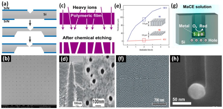
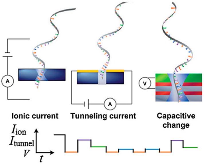
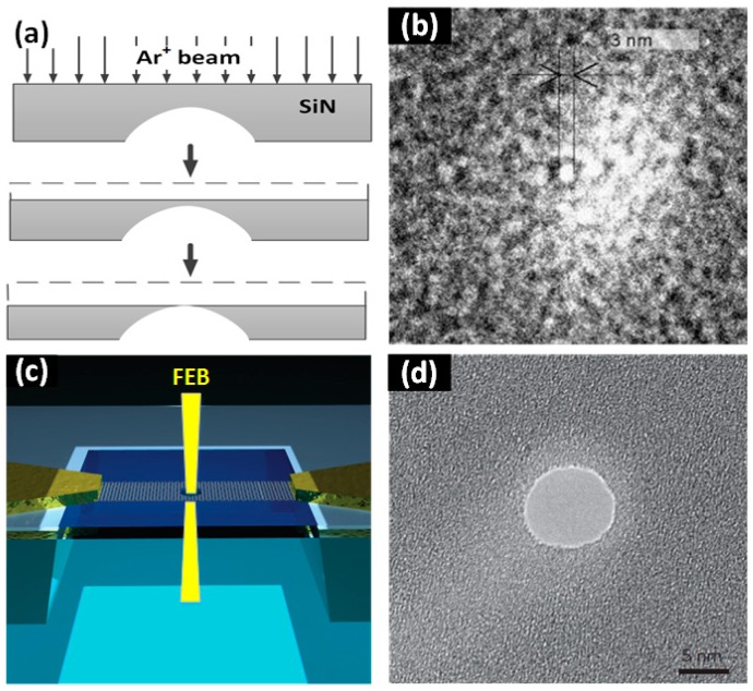
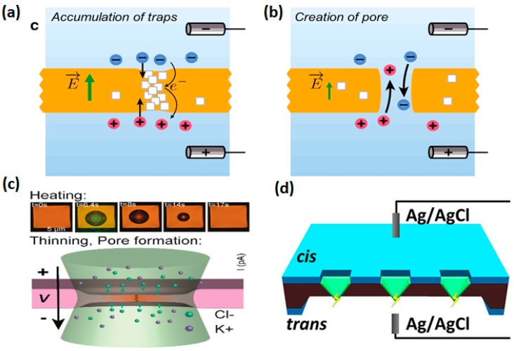
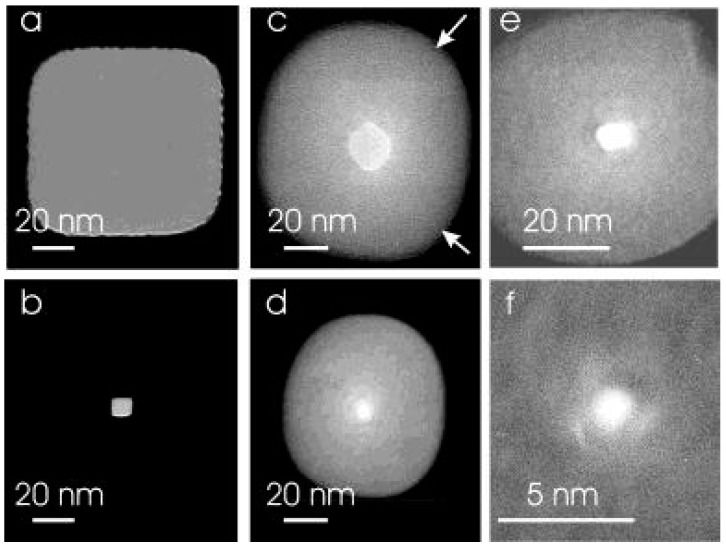
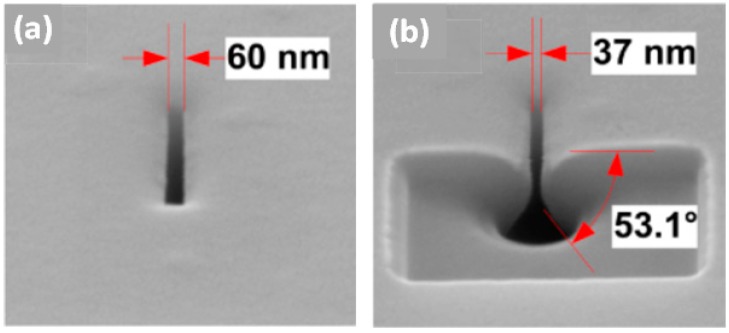
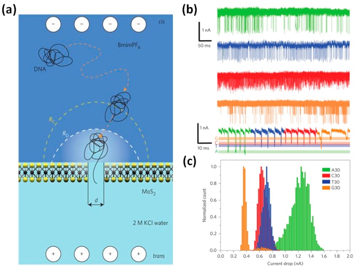
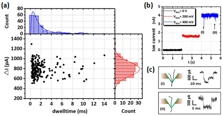
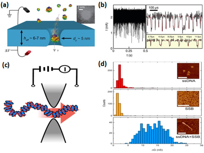
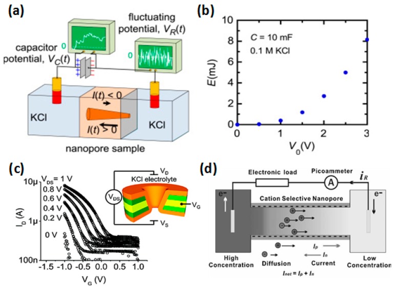
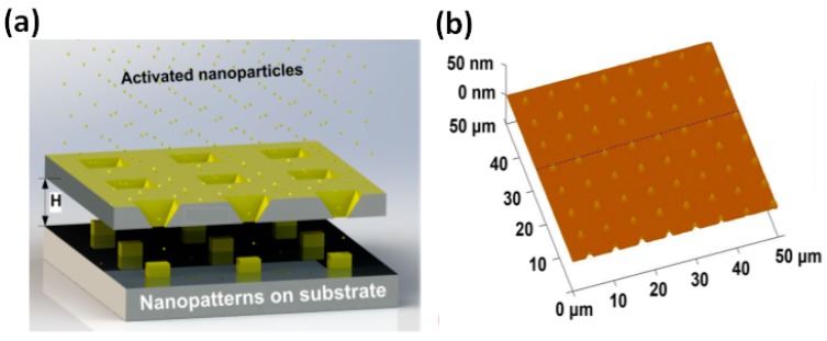
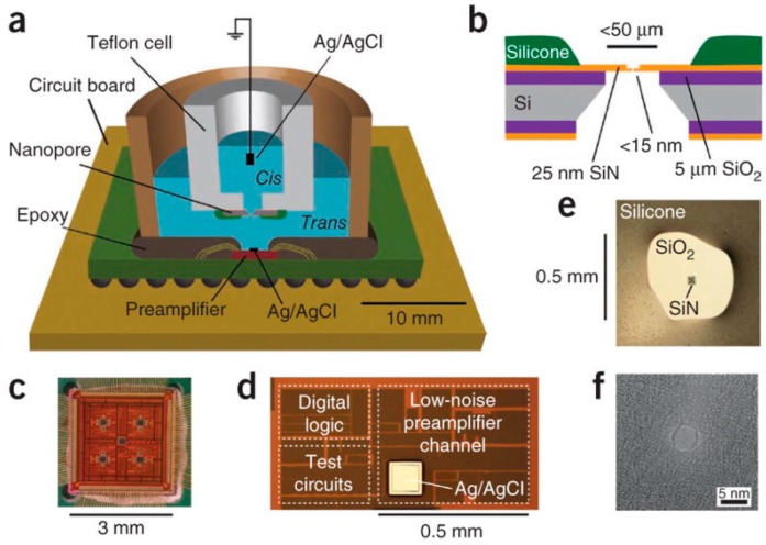
Nanopores fabricated from synthetic materials (solid-state nanopores), platforms for characterizing biological molecules, have been widely studied among researchers. Compared with biological nanopores, solid-state nanopores are mechanically robust and durable with a tunable pore size and geometry. Solid-state nanopores with sizes as small as 1.3 nm have been fabricated in various films using engraving techniques, such as focused ion beam (FIB) and focused electron beam (FEB) drilling methods. With the demand of massively parallel sensing, many scalable fabrication strategies have been proposed. In this review, typical fabrication technologies for solid-state nanopores reported to date are summarized, with the advantages and limitations of each technology discussed in detail. Advanced shrinking strategies to prepare nanopores with desired shapes and sizes down to sub-1 nm are concluded. Finally, applications of solid-state nanopores in DNA sequencing, single molecule detection, ion-selective transport, and nanopatterning are outlined.

Keywords: applications of solid-state nanopores; fabrication and shrinking technologies; solid-state nanopores.


Conflict of interest statement

The authors declare no conflict of interest.

Figures

Figure 4
Figure 4
Chemical solution etching-based fabrication methods. (a) Schematic of the nanopore fabrication process, and (b) a scanning electron microscope (SEM) image of a nanopore array prepared by using the wet etching method (reprinted with permission from [66], copyright 2018, IOP Publishing). (c) Schematic of the track etching method. (d) SEM images of PET membranes with profiled pores (left, cross-sectional morphology of a single pore; right, surface of a membrane with a pore density of 3 × 109 cm−2) (reprinted with permission from [82], copyright 2007, IOP Publishing). (e) Film thickness vs. time during anodization of electropolished aluminum substrates in 0.3 M H2C2O4 (1°C), and (f) an SEM image of Al2O3 nanopore arrays formed by mild anodization (MA) for 2 hours (reprinted with permission from [71], copyright 2006, Springer Nature). (g) Schematic of the Metal-Assisted Chemical Etching (MaCE) technique, and (h) an SEM image of an Si nanopore with a diameter of ~50 nm fabricated by MaCE (reprinted with permission from [84], copyright 2007, Elsevier Ltd.).
Figure 1
Figure 1
Principles of three detection methods of nanopore-based DNA sequencing (reprinted with permission from [22], copyright 2015, Science China Press). The upper panel presents schematics of measurements of the blocked ionic current (left), tunneling current (middle), and capacitive change (right). The lower panel is the time-varying signal.
Figure 2
Figure 2
Focused ion beam (FIB) and focused electron beam (FEB) drilling methods. (a) Schematic of the FIB drilling technique (reprinted with permission from [52], copyright 2001, Springer Nature). (b) A 2.5 nm diameter SiC nanopore fabricated using FIB drilling (reprinted with permission from [46], copyright 2007, Elsevier B.V.). (c) Schematic of the FEB drilling technology. An FEB from the TEM drilled a nanopore directly on a suspended graphene membrane. (d) A TEM image of a graphene nanopore ((c,d) are reprinted with permission from [56], copyright 2013, Springer Nature).
Figure 3
Figure 3
Schematic of the dielectric breakdown method. (a,b) show nanopore formation based on the accumulation of random traps (reprinted with permission from [59]). (c) Photothermally assisted thinning of the SiN membrane to prepare nanopores on a localized heating region (reprinted with permission from [62], copyright 2018, American Chemical Society). (d) Schematic of pore formation at tips of inverted-pyramidal membranes using the high voltage induced dielectric breakdown method (reprinted with permission from [63], copyright 2018, American Chemical Society).
Figure 5
Figure 5
Nanopore arrays fabricated by electron beam lithography (EBL)-assisted fabrication technologies. (a) A nanopore array with an average diameter of 18 ± 2 nm, manufactured using the EBL-assisted RIE method (reprinted with permission from [86], copyright 2014, Royal Society of Chemistry). Ordered Al2O3 nanopores with (b) hexagonal and (c) square shapes prepared by nanoimprinting (reprinted with permission from [89], copyright 2010, American Chemical Society). (d) Nanopore arrays with a sub-10 nm diameter and 40 nm pitch fabricated by nanoimprinting (reprinted with permission from [88], copyright 1997, AIP Publishing).
Figure 6
Figure 6
Metal deposition and the heating induced fabrication method. (a) Schematic and (b) SEM image of pore formation by heating gold patches on the ceramic membrane (reprinted with permission from [91], copyright 2015, American Chemical Society). (c) Schematic of nanopore formation via thermal annealing of gold nanoparticle (AuNP) droplets on the membrane (reprinted with permission from [92], copyright 2018, Royal Society of Chemistry).
Figure 7
Figure 7
(a) Ar ion count rate and nanopore area vs. beam exposure time. Temperature, 28 °C. Flux, 28 Ar+/s/ nm2. Duty cycle, 200 ms/1 s. Energy, 3 keV. (b) TEM image of a nanopore (61 nm in diameter) before shrinking. (c) TEM image of the same sample after Ar+ exposure. The nanopore was shrunk to 1.8 nm (reprinted with permission from [52], copyright 2001, Springer Nature).
Figure 8
Figure 8
The shrinking process of a nanopore under electron beam irradiation from an SEM. The pore was irradiated for (a) 0 s, (b) 100 s, (c) 150 s, (d) 170 s, and (e) 200 s. (f) Nanopore recovery to its original size and shape after oxygen plasma cleaning (reprinted with permission from [102], copyright 2018, IEEE).
Figure 9
Figure 9
TEM images of nanopores before (top row) and after (below row) deposition of Al2O3 coatings by ALD. A square nanopore (a) before and (b) after 500 layers of Al2O3 coating. A circular pore with its initial diameter of 21.6 nm (c) before and (d) after 70 layers of Al2O3 coating to produce a ~4.8 nm pore. A nanopore with its initial diameter of ~7 nm (e) before and (f) after 24 layers of Al2O3 coating to produce a ~2 nm pore (reprinted with permission from [103], copyright 2004, American Chemical Society).
Figure 10
Figure 10
SEM micrographs of a nanopore (a) before and (b) after thermal oxidation-induced shrinkage. FIB cutting was conducted to view the cross-sectional morphology of the shrunk pyramidal nanopore (reprinted with permission from [108], copyright 2013, IOP Publishing).
Figure 11
Figure 11
Identification of single nucleotides in MoS2 nanopores. (a) Schematic of the DNA homopolymer translocation detection. The cis reservoir contains room temperature ionic liquids (BmimPF6) and the trans reservoir contains 2 M aqueous KCl solution. Two reservoirs are separated by a monolayer MoS2 membrane with a nanopore. (b) Translocation signals for each DNA homopolymer in a 2.8 nm MoS2 nanopore: poly A30 (green), poly C30 (red), poly T30 (blue), and poly G30 (orange). (c) Normalized histogram of current drops for each DNA homopolymer (reprinted with permission from [119], copyright 2015, Springer Nature).
Figure 12
Figure 12
Experimental results of λ-DNA translocation through a 5.8 nm nanopore on the pyramidal membrane. (a) Scatter plot of ionic current blockade (ΔI) vs. dwell time (Δt) of double-strand DNA (dsDNA) translocation events. The top figure presents the histogram of Δt, and the right figure shows the histogram of ΔI. (b) Time traces of λ-DNA translocation events through the pore under different applied voltages (Vbias). (c) Schematic and time traces of λ-DNA translocation events in (I) folded and (II) linear modes (reprinted with permission from [63], copyright 2018, American Chemical Society).
Figure 13
Figure 13
Protein detection using solid-state nanopores. (a) Schematic of the protein transport through a 5-nm-diameter HfO2 nanopore. The inset shows the TEM image of the HfO2 pore. (b) Current vs. time trace of the protein at the applied voltage of –125 mV (reprinted with permission from [154], copyright 2014, Elsevier). (c) Schematic of the detection of a single-stranded binding protein (SSB) to ssDNA using a SiN nanopore. (d) Histograms of the mean amplitude of electrical conductance (ΔG) for ssDNA alone (red), SSB alone (yellow), and the mixture of ssDNA with SSB (blue). Insets demonstrate the atomic force microscope images of the respective molecules. Scale bars represent 400 nm (reprinted with permission from [158], copyright 2015, American Chemical Society).
Figure 14
Figure 14
Applications based on ion-selective transport properties of the solid-state nanopores. (a) Schematic of the experimental set-up for energy conversion from fluctuating signals using a conical nanopore. (b) Energy (E) stored in the load capacitor as a function of the noise voltage amplitude (V0) in the 0.1 M KCl solution at C = 1 mF (reprinted with permission from [174], copyright 2015, Elsevier). (c) Log plot of ionic current (ID) vs. the gate voltage (VG) of a nanopore. Inset demonstrates the schematic of the electrode-embedded nanopore (reprinted with permission from [173], copyright 2009, American Chemical Society). (d) Schematic of the generation of net current (Inet) in a solution with a concentration gradient (reprinted with permission from [178], copyright 2010, WILEY-VCH Verlag GmbH & Co. KGaA, Weinheim).
Figure 15
Figure 15
Nanopatterning with solid-state nanopores. (a) Schematic of nanopatterning by the deposition of activated gold-palladium (Au-Pd) nanoparticles on the substrate with a Si nanopore array. (b) An atomic force microscope (AFM) image of a deposited Au−Pd nanocube array with an average planar size of 300 nm (reprinted with permission from [184], copyright 2014, American Chemical Society).
Figure 16
Figure 16
(a) S Schematic of a CMOS-integrated nanopore platform (CNP). (b) Cross-section schematic of the nanopore. (c) Optical micrograph of the 8-channel CMOS current preamplifier. (d) One channel of the preamplifier. (e) Optical image of a SiN nanopore. (f) A TEM image of a SiN nanopore with a diameter of 4 nm (reprinted with permission from [187], copyright 2012, American Chemical Society).

Similar articles

Cited by

References

    1. Kasianowicz J.J., Brandin E., Branton D., Deamer D.W. Characterization of individual polynucleotide molecules using a membrane channel. Proc. Natl. Acad. Sci. USA. 1996;93:13770–13773. doi: 10.1073/pnas.93.24.13770. - DOI - PMC - PubMed
    1. Feng Y., Zhang Y., Ying C., Wang D., Du C. Nanopore-based Fourth-generation DNA Sequencing Technology. Genom. Proteom. Bioinform. 2015;13:4–16. doi: 10.1016/j.gpb.2015.01.009. - DOI - PMC - PubMed
    1. Venkatesan B.M., Bashir R. Nanopore sensors for nucleic acid analysis. Nat. Nanotechnol. 2011;6:615–624. doi: 10.1038/nnano.2011.129. - DOI - PubMed
    1. Miles B.N., Ivanov A.P., Wilson K.A., Doğan F., Japrung D., Edel J.B. Single molecule sensing with solid-state nanopores: Novel materials, methods, and applications. Chem. Soc. Rev. 2012;42:15–28. doi: 10.1039/C2CS35286A. - DOI - PubMed
    1. Clarke J., Wu H.-C., Jayasinghe L., Patel A., Reid S., Bayley H. Continuous base identification for single-molecule nanopore DNA sequencing. Nat. Nanotechnol. 2009;4:265–270. doi: 10.1038/nnano.2009.12. - DOI - PubMed

LinkOut - more resources