. 2019 Apr 30;10(1):1989.
doi: 10.1038/s41467-019-09968-3.

Heteroepitaxial passivation of Cs2AgBiBr6 wafers with suppressed ionic migration for X-ray imaging

Affiliations

Heteroepitaxial passivation of Cs2AgBiBr6 wafers with suppressed ionic migration for X-ray imaging

Bo Yang et al. Nat Commun. .

Abstract

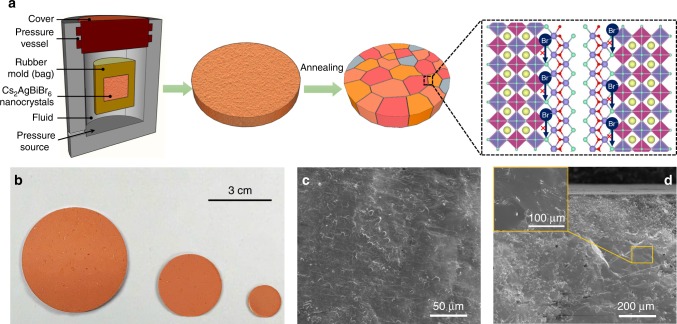
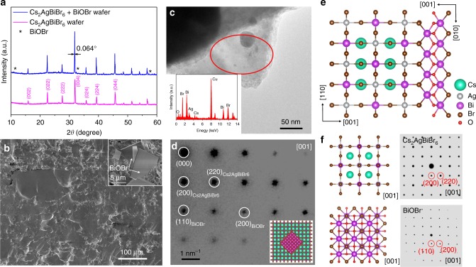
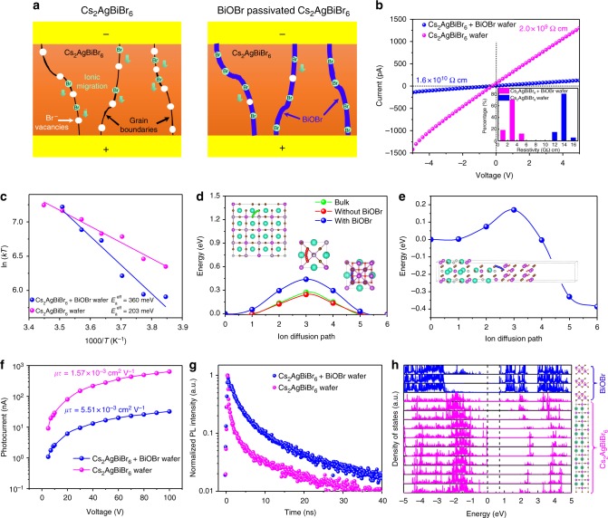
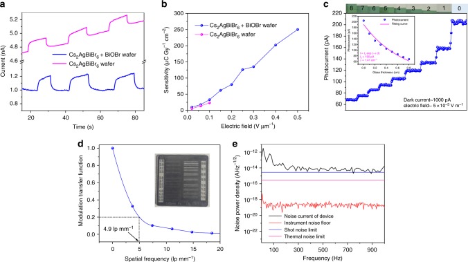
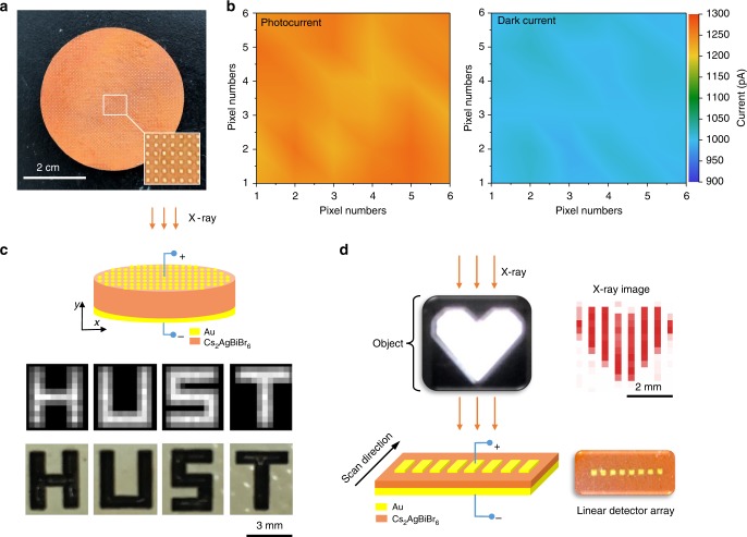
X-ray detectors are broadly utilized in medical imaging and product inspection. Halide perovskites recently demonstrate excellent performance for direct X-ray detection. However, ionic migration causes large noise and baseline drift, limiting the detection and imaging performance. Here we largely eliminate the ionic migration in cesium silver bismuth bromide (Cs2AgBiBr6) polycrystalline wafers by introducing bismuth oxybromide (BiOBr) as heteroepitaxial passivation layers. Good lattice match between BiOBr and Cs2AgBiBr6 enables complete defect passivation and suppressed ionic migration. The detector hence achieves outstanding balanced performance with a signal drifting one order of magnitude lower than all previous studies, low noise (1/f noise free), a high sensitivity of 250 µC Gy air-1 cm-2, and a spatial resolution of 4.9 lp mm-1. The wafer area could be easily scaled up by the isostatic-pressing method, together with the heteroepitaxial passivation, strengthens the competitiveness of Cs2AgBiBr6-based X-ray detectors as next-generation X-ray imaging flat panels.


Conflict of interest statement

The authors declare no competing interests.

Figures

Fig. 1
Fig. 1
Isostatic-pressing method to prepare Cs2AgBiBr6 wafers. a Schematic illustration of the isostatic-pressing process, while Cs2AgBiBr6 powders were firstly modeled into a pie shape and then subsequently subjected to a pressure of 200 MPa through a hydraulic press, and the additional annealing process could enhance the crystallinity and grain growth. b As-prepared Cs2AgBiBr6 wafers with tunable sizes and the diameters are 5, 3, and 1 cm from left to right. c Top–down scanning electron microscopy (SEM) of the wafer. d Cross-sectional SEM image of the wafer and the inset is a higher resolution image, demonstrating the grain size is larger than 100 μm
Fig. 2
Fig. 2
Structural determination of BiOBr-passivated Cs2AgBiBr6 wafer. a XRD spectra of the wafers with/without BiOBr passivation. b Cross-sectional SEM image of the BiOBr-passivated Cs2AgBiBr6 wafer, the inset is the top view. c TEM image of the selected region containing both BiOBr and Cs2AgBiBr6, the inset is the EDS result to verify the presence of Bi, O, Br, Cs, and Ag elements. d SAED pattern of the selected region in c, and the inset is the epitaxial growth model. The corresponding diffraction spots from Cs2AgBiBr6 and BiOBr are labeled accordingly, and the zone axis is [001]. e Epitaxial growth direction between BiOBr and Cs2AgBiBr6. f Crystal structure of Cs2AgBiBr6 and BiOBr viewed from [001] directions and the related diffraction pattern
Fig. 3
Fig. 3
Optical and electrical properties of Cs2AgBiBr6 wafers with/without BiOBr passivation. a Schematic illustration of the suppressed ionic migrations by BiOBr passivation. b The resistivity of the wafers and the inset is the statistical result. c Arrhenius plots of the temperature dependence of kT versus 1000/T, while k is the ionic migration rate (s−1) and is proportional to the ionic conductivity. The fitting curve gives the activation energy of ionic migration, also known as the ion diffusion barriers. d Calculated energy profile along the ionic migration path for VBr (Br vacancies) in bulk Cs2AgBiBr6, in-plane migration for surface of Cs2AgBiBr6 without and with BiOBr passivation. Inset: migration path of VBr with the Br highlighted in green (bulk), red (surface without BiOBr passivation), and blue (surface with BiOBr passivation) color, respectively. e Calculated energy profile of the out-of-plane ionic migration path for the VBr in BiOBr-passivated Cs2AgBiBr6. Inset: Migration path of VBr with the Br highlighted in green, and the VBr migration direction is from BiOBr to Cs2AgBiBr6. f Bias-dependent photoconductivity of the wafers and the derived μτ value. g The time-dependent photoluminescence of the wafers. h Layered decomposed density of states for Cs2AgBiBr6/BiOBr heterostructures
Fig. 4
Fig. 4
Performance of Cs2AgBiBr6 wafer X-ray detector. a Device response to X-rays (138.7 μGyair s−1) under an electric field of 0.1 V μm−1. b X-ray sensitivity under different electric fields. c The response of the detectors toward stacked ITO glass coverslips. d Modulation transfer function for the fabricated detector and the inset is the line pair card for edge spread function measurement. e Measured dark current noise at various frequencies
Fig. 5
Fig. 5
Imaging applications of Cs2AgBiBr6 wafer X-ray detector. a The fabricated multi-pixel wafer-based detector. b Mapping of photocurrent (left) and dark current (right) for the wafer with 6 × 6 pixels as the region of interest. c The Schematic illustration of the imaging process, and the X-ray image (top) and the optical image (bottom) of ‘HUST’ symbol. d Optical image and X-ray image of the heart-shaped logo obtained by the linear detector array, the dose rate for imaging is 138 μGyair s−1, and the scanning mode, as well as the linear detector array is shown at the bottom

References

    1. Yaffe M, Rowlands J. X-ray detectors for digital radiography. Phys. Med. Biol. 1997;42:1. doi: 10.1088/0031-9155/42/1/001. - DOI - PubMed
    1. Yakunin S, et al. Detection of X-ray photons by solution-processed lead halide perovskites. Nat. Photon. 2015;9:444. doi: 10.1038/nphoton.2015.82. - DOI - PMC - PubMed
    1. Wei H, et al. Sensitive X-ray detectors made of methylammonium lead tribromide perovskite single crystals. Nat. Photon. 2016;10:333. doi: 10.1038/nphoton.2016.41. - DOI - PMC - PubMed
    1. Wei W, et al. Monolithic integration of hybrid perovskite single crystals with heterogenous substrate for highly sensitive X-ray imaging. Nat. Photon. 2017;11:315. doi: 10.1038/nphoton.2017.43. - DOI
    1. Shrestha S, et al. High-performance direct conversion X-ray detectors based on sintered hybrid lead triiodide perovskite wafers. Nat. Photon. 2017;11:436. doi: 10.1038/nphoton.2017.94. - DOI

Publication types