

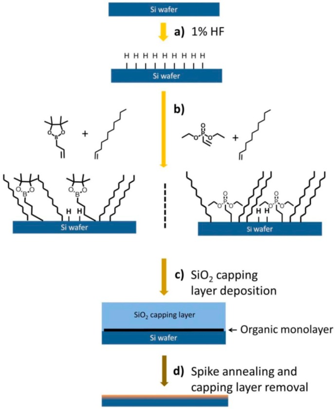
Miniaturization of CMOS
- PMID: 31052223
- PMCID: PMC6563067
- DOI: 10.3390/mi10050293
Miniaturization of CMOS
Abstract
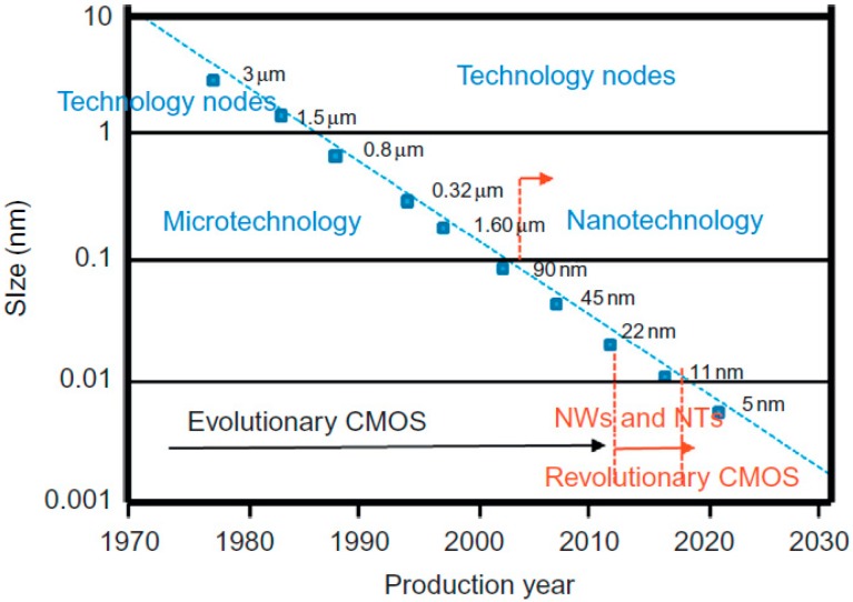
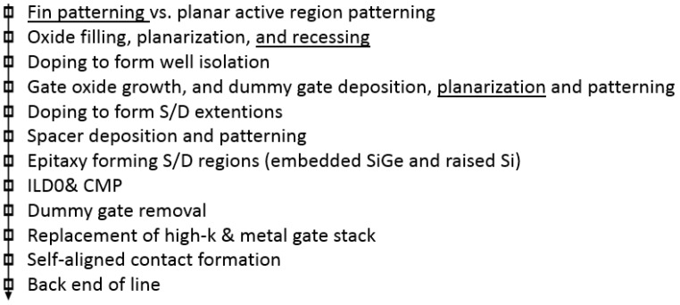
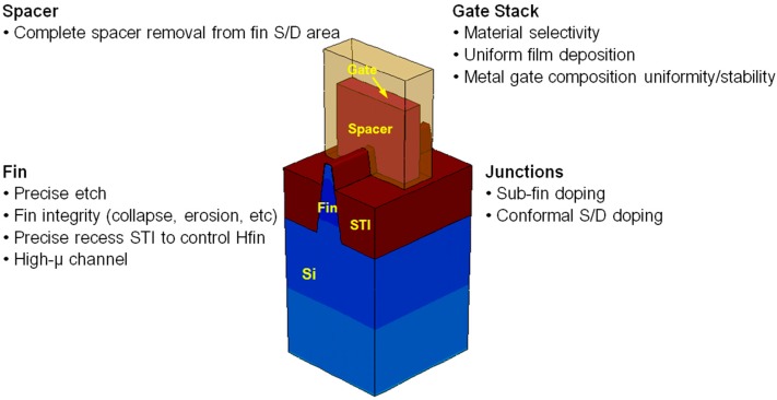
When the international technology roadmap of semiconductors (ITRS) started almost five decades ago, the metal oxide effect transistor (MOSFET) as units in integrated circuits (IC) continuously miniaturized. The transistor structure has radically changed from its original planar 2D architecture to today's 3D Fin field-effect transistors (FinFETs) along with new designs for gate and source/drain regions and applying strain engineering. This article presents how the MOSFET structure and process have been changed (or modified) to follow the More Moore strategy. A focus has been on methodologies, challenges, and difficulties when ITRS approaches the end. The discussions extend to new channel materials beyond the Moore era.
Keywords: CMOS; FinFETs; device processing; integrated circuits.
Conflict of interest statement
The authors declare no conflict of interest.
Figures
References
-
- Moore G.E. Cramming More Components onto Integrated Circuits. Electronics. 1965;38:114. doi: 10.1109/JPROC.1998.658762. - DOI
-
- Colinge J.-P. FinFETs and other Multi-Gate Transistors. Springer; New York, NY, USA: 2008.
-
- Natarajan S., Agostinelli M., Akbar S., Bost M., Bowonder A., Chikarmane V., Chouksey S., Dasgupta A., Fischer K., Fu Q., et al. A 14 nm logic technology featuring 2nd-generation FinFET, air-gapped interconnects, self-aligned double patterning and a 0.0588 µm2 SRAM cell size; Proceedings of the 2014 IEEE International Electron Devices Meeting; San Francisco, CA, USA. 15–17 December 2014; pp. 3–7.
-
- Li C.C., Tsai T.H., Yuan M.S., Liao C.C., Chang C.H., Huang T.C., Liao H.Y., Lu C.T., Kuo H.Y., Hsieh K., et al. A 0.034 mm2, 725 fs RMS jitter, 1.8%/V frequency-pushing, 10.8–19.3 GHz transformer-based fractional-N all-digital PLL in 10 nm FinFET CMOS; Proceedings of the 2016 IEEE Symposium on VLSI Circuits (VLSI-Circuits); Honolulu, HI, USA. 15–17 June 2016; pp. 1–2.
-
- Xu M., Zhu H.L., Zhao L.C., Yin H.X., Zhong J., Li J.F., Zhao C., Chen D.P., Ye T.C. Improved Short Channel Effect Control in Bulk FinFETs with Vertical Implantation to Form Self-Aligned Halo and Punch-Through Stop Pocket. IEEE Electron Device Lett. 2015;36:648–650. doi: 10.1109/LED.2015.2434825. - DOI
Publication types
LinkOut - more resources
Full Text Sources
