Review
. 2017 Oct 23:3:17061.
doi: 10.1038/micronano.2017.61. eCollection 2017.

Advances in diamond nanofabrication for ultrasensitive devices

Affiliations
Review

Advances in diamond nanofabrication for ultrasensitive devices

Stefania Castelletto et al. Microsyst Nanoeng. .

Abstract

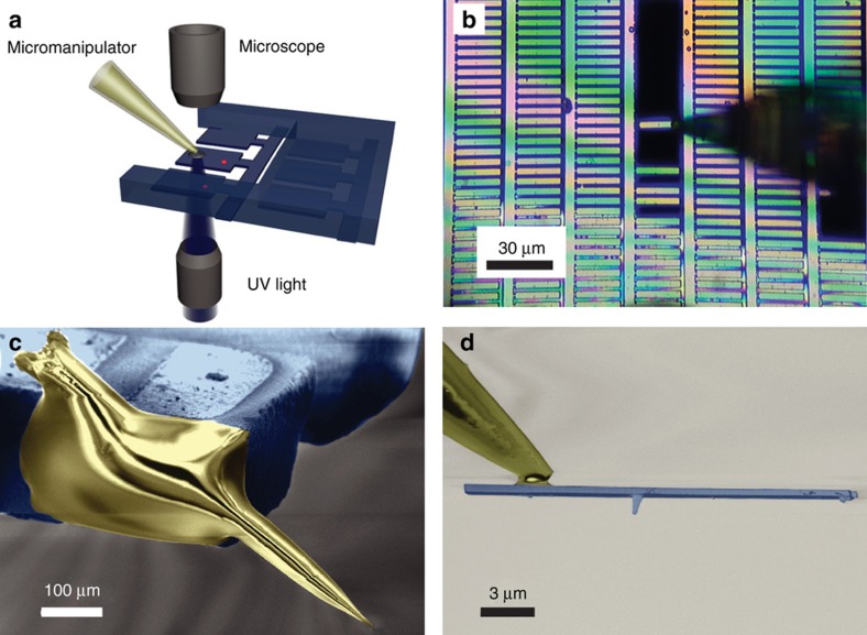
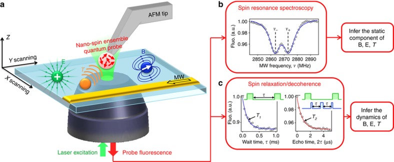
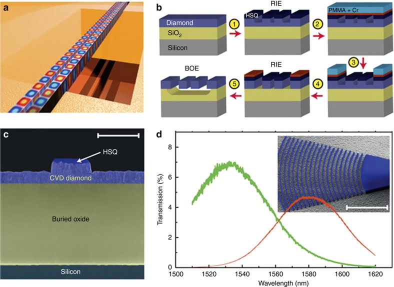
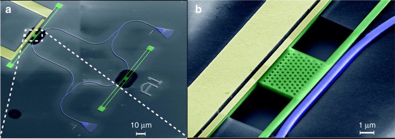
This paper reviews some of the major recent advances in single-crystal diamond nanofabrication and its impact in nano- and micro-mechanical, nanophotonics and optomechanical components. These constituents of integrated devices incorporating specific dopants in the material provide the capacity to enhance the sensitivity in detecting mass and forces as well as magnetic field down to quantum mechanical limits and will lead pioneering innovations in ultrasensitive sensing and precision measurements in the realm of the medical sciences, quantum sciences and related technologies.

Keywords: nano-diamonds; nanofabrication; nanomechanics; nanophotonics; optomechanics.


Conflict of interest statement

The authors declare no conflict of interest.

Figures

Figure 1
Figure 1
(a) Scanning-electron-microscope (SEM) micrographs of 100(25) nm thin and 12 μm wide optical-grade single crystal diamond cantilevers. Image reprinted by permission from Macmillan Publishers Ltd: [Nature Communications]: Ref. , copyright 2014. SEM of diamond doubly clumped nanobeams with width (b) 500 nm, (c) 350 nm, (d) 200 nm and (e) 75 nm. (f) ~3–5 μm diameter undercut micro-disks; and (g) ~500 nm wide nano ring structure. Images reprinted (adapted) with permission from: Ref. . Copyright 2012 American Chemical Society. (h) Atomic force microscopy (AFM) image of a focused-ion-beam (FIB)-defined dome, scan size 5·5 μm2. Inset shows an electron backscatter diffraction (EBSD) pattern confirming the single-crystal nature of the device layer. Image reprinted with permission from: Ref. . Copyright 2011 American Chemical Society). (i) Regular array of lithographically defined single crystal diamond tips (scale bar, 10 μm) and (ii) zoom in after cleavage resulting in sharp tips with radii of about 10 nm. The scale bar is 100 nm. Images reprinted (adapted) with permission from: Ref. . Copyright 2015 American Chemical Society.
Figure 2
Figure 2
Data from Refs. , showing f, Qm and fc·Qm versus the length for single clamped nanobeams single crystal diamond measured at room temperature in vacuum.
Figure 3
Figure 3
(a) Measured Qm values for different temperatures, cantilever lengths and materials: single crystal diamond (SCD) in electronic-grade (EG) and optical-grade (OG), polycrystalline diamond (PCD) and single-crystal Silicon (Si). Arrows indicate record Qm reported in the text. (b) Inferred and projected sensitivities for force measurement of different cantilevers versus temperature and thickness for B=1 Hz. Data from Refs. ,,,,,. The arrows indicate current best realization with diamond and silicon, while the circles indicate the required sensitivity for nuclear magnetic resonance signals using spin magnetic resonance force microscopy. Experiments in the range 3 K to 300 K show that EG SCD gives Qm factors up to one order of magnitude higher than optical-grade single crystal diamond, comparing cantilevers of similar thickness (100–300 nm).
Figure 4
Figure 4
Scanning electron microscopy images of: (a) Diamond nanopillars fabricated on a (111)-oriented single-crystalline diamond sample. Image reprinted from Ref. with the permission of AIP Publishing. (b) An array of waveguide-coupled single crystal diamond ring resonators on a SiO2/Si substrate obtained by the thin-down and electron beam lithography (EBL) techniques. The rings are 850 nm high and 875 nm wide and have radii of 20–30 μm with record Q-factor~106 at λ=1545 nm. Images reprinted by permission from Macmillan Publishers Ltd: Nature Photonics. Ref. , copyright 2014. (c) 7.9 μm diameter microdisk in a diamond chip with 〈100〉-oriented surface and edge crystal planes fabricated by undercut and EBL techniques, Q~115 000 at λ =1552 nm. Image reprinted (adapted) with permission from Ref. . Copyright 2015 American Chemical Society. (d) 1D nano-beam cavity with width ~1 μm, fabricated by angle-etching method and EBL techniques, resonant at λ=1, 680 nm, made of elliptical holes with lattice constant ~536 nm and radius of the holes ~146 nm. The record loaded Q~183000. Image reprinted by permission from Macmillan Publishers Ltd: Nature Communications: Ref. , copyright 2014. (e) Linear three-hole defects 2D-PHC cavity fabricated in a triangular lattice with period a~218 nm, hole radius r=0.29·a~63 nm, and membrane thickness h=0.91·a~198 nm, optical Q-factor~3000 and λ=637 nm. Fabricated by thin-down technique using reactive ion etching and EBL. Image reprinted figure with permission from: Ref. . Copyright 2012 by the American Physical Society.
Figure 5
Figure 5
Optical Q-factors measured for different optical resonators and expected maximum enhancement based on the mode volume design Fp, max he cavity coupled with color centres are indicated with star. Data from Refs. ,,,,,,. We observe that the experimental Q-factors generated when the same cavity is coupled to a color center tend to be much smaller compared to an unloaded cavity and the FSE tends to be much smaller compared to the expected Fp, max. By way of an example in Ref. a measured loaded Q-factor of 3000 (theoretical Q=6000) is achieved with a record FSE=70, while the expected Fp, max~260 based on the cavity mode volume. In Ref. FSE=63 while the expected Fp, max~194.
Figure 6
Figure 6
Examples of diamond nanofabrication and patterning. (a) Dry etching (oxygen plasma in an Oxford RIE etching machine) thin-down technique of 5 μm-thick diamond membrane until it is 300 nm thick placed on a 2 μm-thick SiO2 layer grown on a silicon wafer. The electron-beam resist (Fox12) is spun on the chip and electron-beam lithography used to pattern a ring resonator. The pattern is transferred from the resist to the diamond using dry etching in an oxygen plasma. Image available under the terms of the Creative Commons Attribution 3.0 License from Ref. . (b) Process for fabrication of diamond nanobeams using quasi-isotropic reactive-ion undercut etching. Image available under the terms of the Creative Commons Attribution 3.0 License from Ref. . (c) Patterning of a diamond membrane using a silicon membrane as a contact etch mask. (I) Transferring of a Si mask onto a <300 nm diamond membrane using a micro PDMS adhesive. (II) The silicon membrane on top of the diamond membrane is used as an etch mask for oxygen plasma etching. (III) The diamond membrane is patterned during oxygen etching with subsequent mask removal. (IV) A SF6 isotropic dry etching removed the silicon underneath and suspended the diamond membrane. Image reprinted by permission from Macmillan Publishers Ltd: [Scientific Reports]: Ref. , copyright 2015.
Figure 7
Figure 7
(a) 1D PhC cavities integrated on a Si substrate with metallic strip lines to provide microwave excitation for NV-center coherent spin control. The cavity is a rectangular nanobeam based on a suspended 1D diamond PHC structure with a lattice constant a=220 nm, beam width W=2.4·a and a thickness of h=0.7·a. The inset shows the NV-nano cavity system with the NV-nano cavity coupling g, γ is the NV natural SE decay rate and k is the cavity intensity decay rate. The defect was positioned in the cavity by 15N-ions implantation and subsequent annealing at 850 °C. (b) Simulated electric field intensity for the optimized fundamental cavity mode showing high confinement at the center of the cavity. (c) Scanning electron microscope (SEM) of a representative cavity structure. The scale bar represents 1 μm. (d) Measured cavity resonance with a quality factor Q~9, 900±200. Images reprinted by permission from Macmillan Publishers Ltd: Nature Communications: Ref. , copyright 2015.
Figure 8
Figure 8
(a) Scanning electron microscope (SEM) micrograph of the diamond cavity (scale bar corresponds to 1 μm). (b) Focused ion beam (FIB) cross-section of a photonic crystal region (scale bar corresponds to 200 nm). The diamond-nanopillars are arranged in a hexagonal lattice, with a center-to-center spacing, a. The center of the lattice contains a linear defect, made up of three conjoined neighboring rods from the lattice, each with a radius of R, such that the length of the cavity is L=2·(R+a). The images are reprinted (adapted) with permission from: Ref. . 2015 American Chemical Society.
Figure 9
Figure 9
(a) The all-diamond scanning probe made of diamond cantilevers with diamond nanopillar are glued to a quartz tip. (b) Optical microscope image during the transfer process of the diamond probe to the atomic force microscopy (AFM) head. (c) Scanning electron microscope (SEM) image of the scanning probe attached to an AFM tuning fork. (d) SEM image of the final scanning probe attached to the end of the quartz tip. The cantilever was 20 μm long, 3 μm wide and connected to the diamond substrate via 500 nm bridges. The NV-center was created by 14N implantation at a depth of only 9 nm, reaching a trade-off with a spin coherence time of 76 μs (a shallow depth gives higher resolution, but also shorter coherence time due to proximal surface spins, and thus, lower sensitivity). Images reprinted from: Ref. , with the permission of AIP Publishing.
Figure 10
Figure 10
Schematic of the scanning nano-spin ensemble microscope. (a) Probe consists of a nano-diamond containing a small ensemble of electronic spins (symbolized by the red arrows) grafted onto the tip of an atomic force microscope (AFM). Optical excitation and readout, combined with microwave (MW) excitation, enable quantum measurements of the spin ensemble properties, such as spin resonance, relaxation and decoherence. Scanning the sample relative to the probe produces images of the sample with magnetic (B field), electric (E field) or temperature (T) contrasts, depending on the probing technique used. (b) Optically detected spin resonance spectrum of a nano-diamond on a tip. The solid line is the fit to a sum of two Lorentzian functions centered at frequencies ν±=D±E, providing the zero-field splitting parameters D=2868.3±0.1 MHz and E=5.4±0.1 MHz. (c) Spin relaxation (left) and spin decoherence (right) curve of a nano-diamond on the AFM tip. The inset depicts the sequence of laser (green) and MW (blue) pulses employed. Solid lines are fits to a single exponential decay, revealing a spin relaxation time of T1=142±9 μs and a spin coherence time of T2=780±30 ns. Images reprinted with permission from: Ref. , Copyright 2016 American Chemical Society.
Figure 11
Figure 11
Diamond optomechanical resonators. (a) Schematic of coupled free-standing waveguides, which act as mechanical resonators. Propagating optical modes are overlaid in color. (b) Fabrication routine used to prepare both photonic circuitry and mechanical elements on-chip. (c) Cross-sectional scanning electron microscope (SEM) image of a diamond nano photonic ridge waveguide. Individual layers are marked in false-color. Scale bar, 1 mm. (d) Transmission curves of diamond waveguides connected to focusing grating couplers (inset: SEM image of a fabricated device, scale bar, 7.5 mm). The central coupling wavelength is tuned by adjusting the period of the grating. Images reprinted by permission from Macmillan Publishers Ltd: Nature Communications: Ref. . Copyright 2013.
Figure 12
Figure 12
False color scanning electron microscope-micrographs of a fabricated electro-optomechanical device. (a) The integrated Mach-Zehnder interferometer is shown in blue. The mechanical resonator, which is evanescently coupled to the waveguide, is shown in green, while the metal electrodes are shown in golden color. (b) Detailed view of the free-standing resonator. The photonic crystal mirror separates the optical components from the electrode section. Images reprinted from Ref. , with the permission of AIP Publishing.

References

    1. Rath P, Ummethala S, Nebel C et al. Diamond as a material for monolithically integrated optical and opto mechanical devices. Physica Status Solidi A Applications and Materials Science 2015; 212: 2385–2399.
    1. Ekinci KL, Roukes ML. Nanoelectromechanical systems. Review of Scientific Instruments 2005; 76: 061101.
    1. Greentree AD, Fairchild BA, Hossain FM et al. Diamond integrated quantum photonics. Materials Today 2008; 11: 22–31.
    1. Aharonovich I, Greentree AD, Prawer S. Diamond photonics. Nature Photonics 2011; 5: 397–405.
    1. Popovich AF, Ralchenko VG, Balla VK et al. Growth of 4'' diameter polycrystalline diamond wafers with high thermal conductivity by 915 MHz microwave plasma chemical vapor deposition. Plasma Science and Technology 2017; 19: article no. 035503.