. 2019 May;569(7755):208-214.
doi: 10.1038/s41586-019-1157-8. Epub 2019 May 8.

All-optical spiking neurosynaptic networks with self-learning capabilities

Affiliations

All-optical spiking neurosynaptic networks with self-learning capabilities

J Feldmann et al. Nature. 2019 May.

Abstract

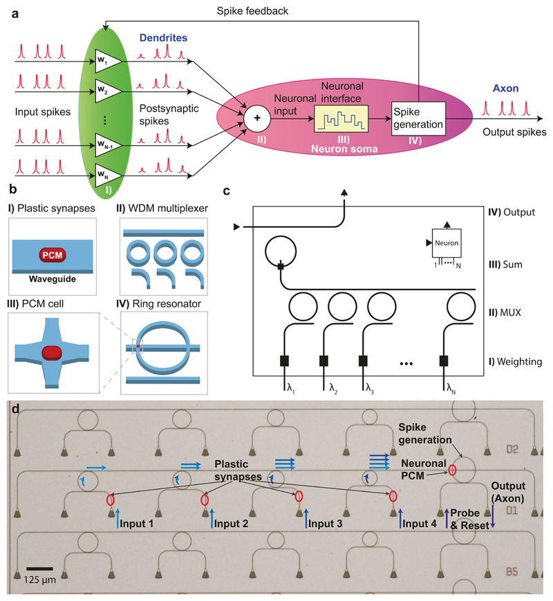
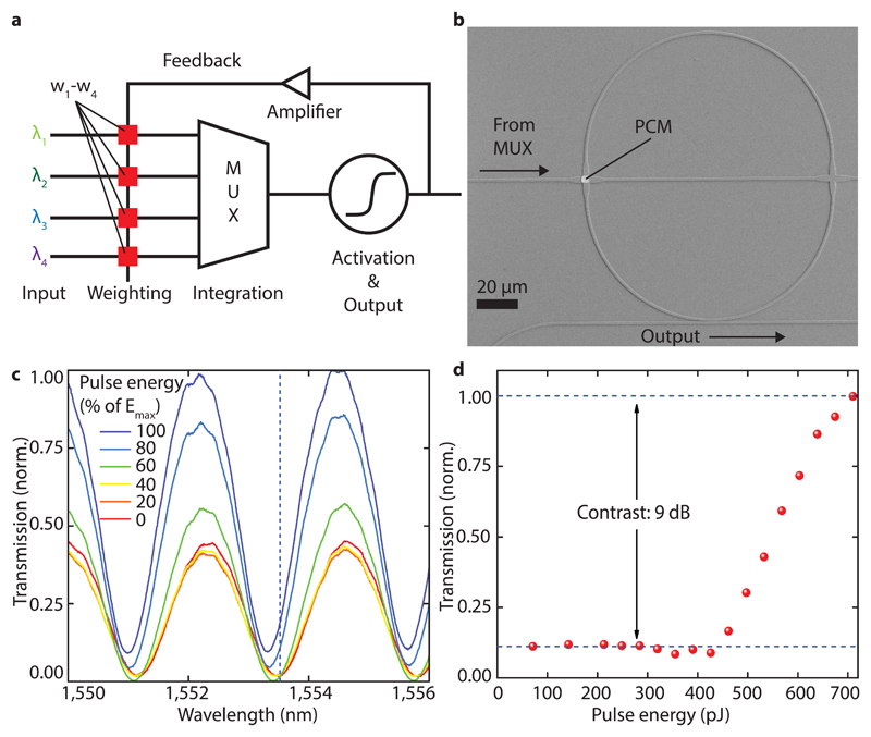
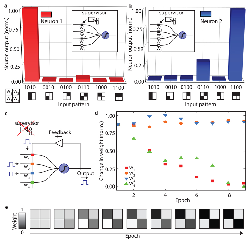
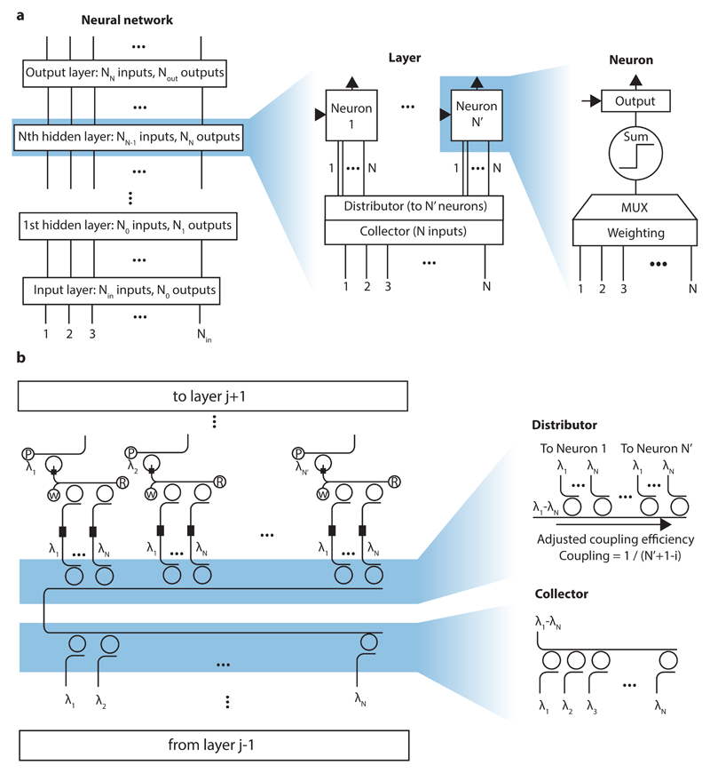
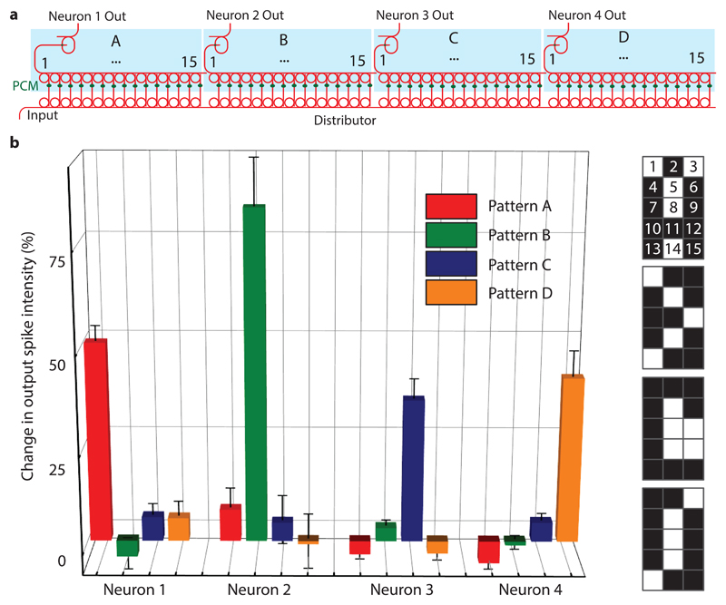
Software implementations of brain-inspired computing underlie many important computational tasks, from image processing to speech recognition, artificial intelligence and deep learning applications. Yet, unlike real neural tissue, traditional computing architectures physically separate the core computing functions of memory and processing, making fast, efficient and low-energy computing difficult to achieve. To overcome such limitations, an attractive alternative is to design hardware that mimics neurons and synapses. Such hardware, when connected in networks or neuromorphic systems, processes information in a way more analogous to brains. Here we present an all-optical version of such a neurosynaptic system, capable of supervised and unsupervised learning. We exploit wavelength division multiplexing techniques to implement a scalable circuit architecture for photonic neural networks, successfully demonstrating pattern recognition directly in the optical domain. Such photonic neurosynaptic networks promise access to the high speed and high bandwidth inherent to optical systems, thus enabling the direct processing of optical telecommunication and visual data.


Conflict of interest statement

Competing interests

The authors declare no competing interests.

Figures

Figure 1
Figure 1. All-optical spiking neuronal circuits.
a-b) Schematic of the network realized in this work consisting of several pre-synaptic input neurons and one post-synaptic output neuron connected via PCM-synapses. The input spikes are weighted using PCM-cells and summed up using a WDM multiplexer. If the integrated power of the postsynaptic spikes surpasses a certain threshold, the PCM-cell on the ring resonator switches and an output pulse (neuronal spike) is generated. c) Photonic circuit diagram of an integrated optical neuron with symbol block shown in the inset (top right). Several of these blocks can be connected to larger networks using the wavelengths inputs and outputs as described in more detail in Figure 5 d) Optical micrograph of three fabricated neurons (B5, D1 and D2) showing four input ports. The four small ring resonators on the left are used to couple light of different wavelengths from the inputs to a single waveguide, which then leads to the phase-change material cell at the crossing point with the large ring. The triangular structures on the bottom are grating couplers used to couple light onto and off the chip.
Figure 2
Figure 2. Spike generation and operation of the artificial neuron.
a) Schematic of the photonic implementation of a phase-change neuron circuit. Light of different wavelength is weighted by phase-change elements w1-w4 and summed up by a multiplexer to a single waveguide. If this activation energy surpasses a threshold, an output pulse is generated, and the weights are updated. b) Scanning electron micrograph of a ring resonator used to implement the activation function. By switching the PCM-cell on top of the waveguide crossing, the resonance condition of the resonator can be tuned. The waveguide on the bottom of the ring is used to probe the resonance and generate an output pulse. c) Transmission measurement of the device in b) and its dependence of pulse energy. The resonance shifts towards shorter wavelength with increasing pulse energy send to the PCM-cell on the ring. At the same time the transmission increases because of reduced absorption in the PCM-cell and thus changes the coupling between ring and waveguide. d) Normalized transmission to the output at a fixed wavelength (dashed line in c)) showing the activation function used to define the firing threshold of the neuron.
Figure 3
Figure 3. Supervised and unsupervised learning with phase-change all-optical neurons.
a) and b) show the neuron output of two individual neurons when presented with different input patterns. Neuron one learned to recognize pattern ‘1010’, while neuron two generates an output signal when ‘1100’ is shown. In this example the eight weights of the neural network were set by an external supervisor. c) Schematic illustrating the unsupervised learning mechanism in an all-optical neuron. If an output spike is generated, the synaptic-weights where input and feedback pulses overlap in time are potentiated, while the weights that are only hit by the single feedback pulse are depressed. d) Change of the four synaptic weights over time when the pattern ‘0110’ is repeatedly shown starting from fully amorphous (high transmitting) weights. The weights where input- and feedback pulse overlap stay almost constant over several epochs. The other weights where only the feedback pulse is shown decrease continuously. e) Development of the weights over time, clarifying that the information of the pattern is encoded in the weights.
Figure 4
Figure 4. Scaling architecture for all-optical neural networks.
a) The general neural network is composed of an input layer, an output layer and several hidden layers. Each of these layers consist of a collector gathering the information from the previous layer, a distributor that equally splits the signal to individual neurons and the neuronal and synaptic elements of the layer itself. Each neuron has a weighting unit and a multiplexer to calculate the weighted sum of the inputs. The sum is then fed to an activation unit which decides if an output pulse is generated. b) Photonic implementation of a single layer from the network. The collector unites the optical pulses from the previous layer using a WDM multiplexer. A distributor made from the same rings as the collector but with adjusted coupling efficiency equally distributes the input signal to the PCM synapses of each neuron. The letters “P”, “W” and “R” denote the input ports used to probe the output, set the weights and return the neuronal PCM to its initial state.
Figure 5
Figure 5. Experimental realisation of a single layer spiking neural network.
a)The device consists of four photonic neurons, each with 15 synapses. Each synapse corresponds to a pixel in a 3x5 image (see b)) and is encoded in the wavelengths corresponding to the ring multiplexers (see numbering in b)). The full device comprises an integrated photonic circuit built up from 140 optical components. b) The change in output spike intensity is shown for the four trained patterns illustrated on the right-hand side. The neural network successfully recognizes the four patterns as each neuron only responds (spikes) to one of the patterns. The error bars denote the standard deviation for n=5.

Comment in

References

    1. Lane ND, et al. Squeezing Deep Learning into Mobile and Emdedded Devices. IEEE Pervasive Comput. 2017;16:82–88.
    1. Amato F, et al. Artificial neural networks in medical diagnosis. J Appl Biomed. 2013;11:47–58.
    1. Nawrocki RA, Voyles RM, Shaheen SE. A Mini Review of Neuromorphic Architectures and Implementations. IEEE Trans Electron Devices. 2016;63:3819–3829.
    1. Preissl R, et al. Compass: A scalable simulator for an architecture for cognitive computing. Int Conf High Perform Comput Networking, Storage Anal SC; 2012.
    1. von Neumann J. The Computer and The Brain. Yale University Press; 1958.

Publication types