

Evaluation of CdZnTeSe as a high-quality gamma-ray spectroscopic material with better compositional homogeneity and reduced defects
- PMID: 31086249
- PMCID: PMC6513868
- DOI: 10.1038/s41598-019-43778-3
Evaluation of CdZnTeSe as a high-quality gamma-ray spectroscopic material with better compositional homogeneity and reduced defects
Abstract
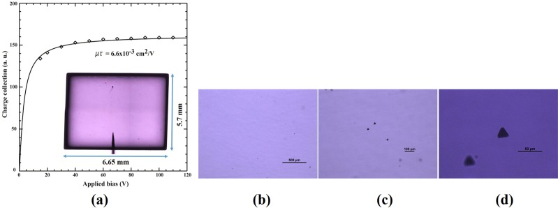
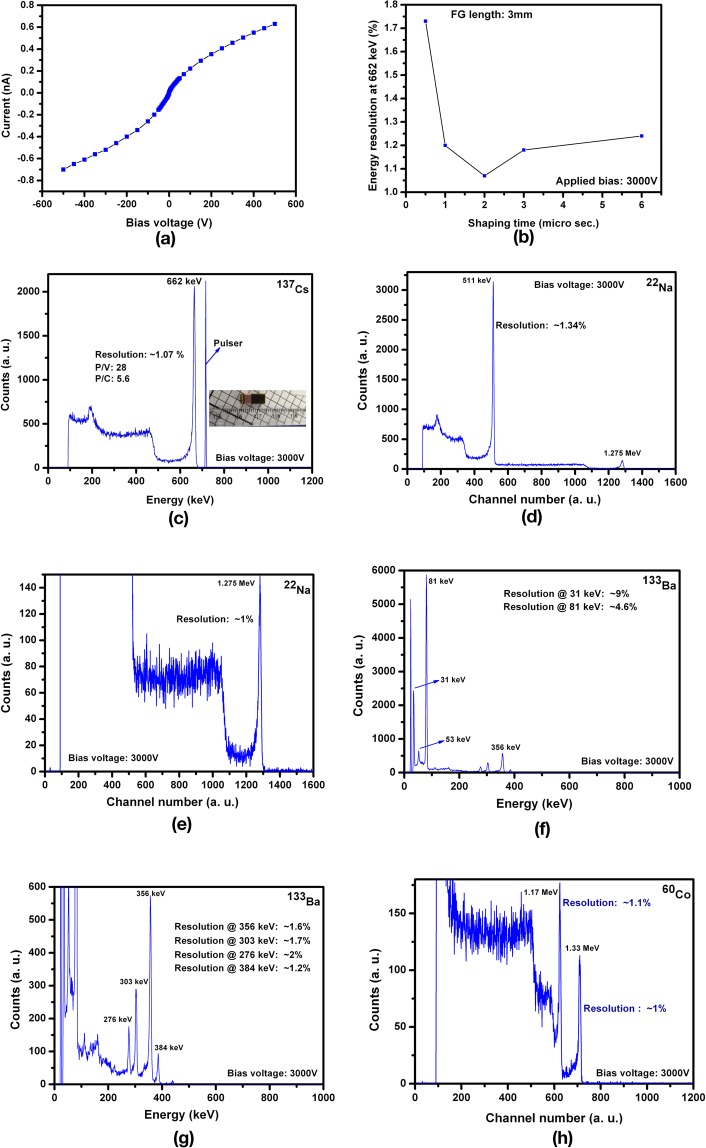
X- and gamma-ray detectors have broad applications ranging from medical imaging to security, non-proliferation, high-energy physics and astrophysics. Detectors with high energy resolution, e.g. less than 1.5% resolution at 662 keV at room temperature, are critically important in most uses. The efficacy of adding selenium to the cadmium zinc telluride (CdZnTe) matrix for radiation detector applications has been studied. In this paper, the growth of a new quaternary compound Cd0.9Zn0.1Te0.98Se0.02 by the Traveling Heater Method (THM) is reported. The crystals possess a very high compositional homogeneity with less extended defects, such as secondary phases and sub-grain boundary networks. Virtual Frisch-grid detectors fabricated from as-grown ingots revealed ~0.87-1.5% energy resolution for 662-keV gamma rays. The superior material quality with a very low density of defects and very high compositional homogeneity heightens the likelihood that Cd0.9Zn0.1Te0.98Se0.02 will be the next generation room-temperature detector material.
Conflict of interest statement
The authors declare no competing interests.
Figures

References
-
- Schlesinger TE, et al. Cadmium zinc telluride and its use as a nuclear radiation detector material. Materials Science and Engineering. 2001;R 32:103. doi: 10.1016/S0927-796X(01)00027-4. - DOI
-
- Yang, G. & James, R. B. Physics, Defects, Hetero- and Nano-structures, Crystal Growth, Surfaces and Applications Part II, (EDAX. Triboulet R. et al.) 214 (Elsevier, 2009).
-
- Wilson MD, et al. A 10 cm × 10 cm CdTe Spectroscopic Imaging Detector based on the HEXITEC ASIC. J. Instrumentation. 2015;10:10011. doi: 10.1088/1748-0221/10/10/P10011. - DOI
-
- Iniewski K. CZT sensors for Computed Tomography: from crystal growth to image quality, J. Instrumentation. 2016;11:C12034. doi: 10.1088/1748-0221/11/12/C12034. - DOI
-
- Burger A, et al. Development of portable CdZnTe spectrometers for remote sensing of signatures from nuclear materials. Phys. Status Solidi. 2005;C2:1586. doi: 10.1002/pssc.200460839. - DOI
LinkOut - more resources
Full Text Sources
