. 2019 May 17;5(5):eaav2252.
doi: 10.1126/sciadv.aav2252. eCollection 2019 May.

Engineering single-atom dynamics with electron irradiation

Affiliations

Engineering single-atom dynamics with electron irradiation

Cong Su et al. Sci Adv. .

Abstract

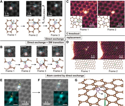
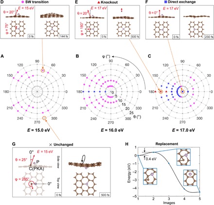
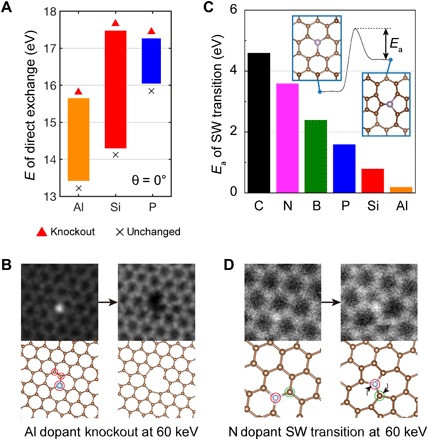
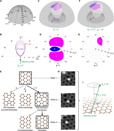
Atomic engineering is envisioned to involve selectively inducing the desired dynamics of single atoms and combining these steps for larger-scale assemblies. Here, we focus on the first part by surveying the single-step dynamics of graphene dopants, primarily phosphorus, caused by electron irradiation both in experiment and simulation, and develop a theory for describing the probabilities of competing configurational outcomes depending on the postcollision momentum vector of the primary knock-on atom. The predicted branching ratio of configurational transformations agrees well with our atomically resolved experiments. This suggests a way for biasing the dynamics toward desired outcomes, paving the road for designing and further upscaling atomic engineering using electron irradiation.


Figures

Fig. 1
Fig. 1. Illustration of competing experimental P dopant dynamics in graphene and its control.
The frames are medium-angle annular dark-field images, and the chemical identity of each dopant was confirmed by electron energy-loss spectroscopy (EELS). (A) Three frames showing a direct exchange between the brighter (due to its greater scattering contrast) P atom and a C neighbor, with the initial (frame 1), transition (frame 2), and final configurations (frame 3). White and black dashed lines indicate the row of the scanning beam when the exchange happens. Scan speed, 8.4 s per frame. No postprocessing was done. (B) Four frames showing both direct exchange (frames 1 and 2) and SW transition (frames 2 to 4). Scale bars, 2 Å. Scan speed, 0.07 s per frame. A median filter with a 2 pixel × 2 pixel kernel was applied for clarity. The SW transition was captured during EELS acquisition in small subscan windows to enhance the signal-to-noise ratio of the spectra used to identify the dopants and to achieve faster scanning rate frames that can better capture atomic dynamics. (C) Neighboring C atom knocked out by the electron beam, turning a threefold-coordinated P into fourfold-coordinated P. Scan speed, 8 s per frame. No postprocessing was done. (D) P dopant being replaced by a C atom. Scan speed, 4 s per frame. The different image color codings represent different categories: gray represents atom-conserving process, and magenta represents atom-nonconserving process. Blue and red dashed circles in (A) and (B) represent the inequivalent lattice sites of graphene, and the green dashed circles in (C) and (D) indicate the location of the atom that has not been conserved. (E and F) Intentional control over the P direct exchange. The yellow crosses indicate the location where the electron beam was parked for 10 s to purposefully move the P atom by one lattice site. Green and blue dashed circles indicate the two nonequivalent lattices sites of graphene. Insets: The region of interest after applying a Gaussian filter. (G) A schematic plot of the control process, where the electron beam is represented by a green cone focused on the neighbor C atom.
Fig. 2
Fig. 2. Mechanisms of P dopant dynamics in graphene calculated with abMD.
(A to C) Angular distribution maps of different possible lattice transformations obtained when a C neighbor of the P impurity is given an initial out-of-plane momentum. The corresponding initial kinetic energies on the carbon, E, are (A) 15.0, (B) 16.0, and (C) 17.0 eV. The marks in these polar plots indicate the dynamical outcome: C knockout as red triangles, direct exchange as blue squares, SW transitions as magenta circles, and unchanged lattice as black crosses. As examples, snapshots of (D) SW transition (θ = 20°, φ = 75°, E = 15.0 eV), (E) C knockout (θ = 20°, φ = 180°, E = 17.0 eV), (F) direct exchange (θ = 0°, E = 17.0 eV), and (G) unchanged structure (θ = 25°, φ = 285°, E = 15.0 eV) are shown. The red arrows indicate the direction of the C momentum along the in-plane and normal-to-plane directions (lengths not to scale), with the definition of the spherical coordinate angles θ and φ shown in (G). (H) cNEB barrier for a proposed mechanism of P dopant replacement by C. Insets: The initial, saddle-point, and final configurations.
Fig. 3
Fig. 3. Comparison of dynamics of different impurity elements.
(A) Comparison of the direct exchange energy ranges between Al, Si, and P for head-on collision (θ = 0°). (B) Experimentally, the knockout of an Al dopant and two carbon atoms nearby was observed after 7 min of continuous radiation at 60 keV, corresponding to the low displacement threshold predicted in (A). Red circles mark atoms displaced in the second frame. (C) The energy barriers (Ea) of configurational change from 55-77 structures back to the pristine lattice are illustrated for various elements (C, 4.6 eV; N, 3.6 eV; B, 2.4 eV; P, 1.6 eV; Si, 0.8 eV; Al, 0.2 eV). Inset: The definition of Ea in the energy profile of the SW transition, where the original curves can be found in fig. S4. (D) An experimentally observed SW transition of an N dopant at 60 keV.
Fig. 4
Fig. 4. PKS: A scheme for evaluating cross sections of different dynamic processes.
(A) The spherical coordinate system used for describing the PKS (with θ and φ defining the direction of momentum, and the radius defining the postcollisional kinetic energy, E, of the C neighbor). (B) A vertical cross section of the PKS showing the distribution of function f (dubbed “ovoid” hereafter) for the upward 60-keV electron beam (θ˜e=0°) interacting with a moving PKA (E˜=0 to 1 eV). (C) The ovoid of a vibrational PKA (we use E˜=0.5 eV here for the amplified illustration) intersects with different outcome areas, where in (D), the intersections are projected to a polar plot. The magenta areas marked with a and c represent SW transitions (clockwise and counterclockwise, respectively), and the blue area marked with b represents direct exchange. (E) A decision tree showing possible outcomes of the atom-electron interaction, where the probability of going through each path is proportional to the cross sections. (F) The PKS and the ovoid of a tilted electron beam (θ˜e=17.2°,φ˜e=15°) acting on a vibrational PKA (E˜=0.5 eV), with (G) showing a different intersection projected to the polar plot. Here, only clockwise SW transitions are activated, marked with d in the magenta area. (H) An experimentally observed clockwise SW transition of a Si dopant activated in a tilted sample as in (F) and (G). Three corresponding stages are placed alongside the decision tree in (E), where the experimental states are marked by black squares, and the observed path is indicated by the thicker branches. Field of view: 1 nm × 1 nm. (I) A side perspective view of the electron beam tilted with respect to the graphene plane. The sample was kept tilted like this throughout all the frames in (H).

References

    1. Ishikawa R., Mishra R., Lupini A. R., Findlay S. D., Taniguchi T., Pantelides S. T., Pennycook S. J., Direct observation of dopant atom diffusion in a bulk semiconductor crystal enhanced by a large size mismatch. Phys. Rev. Lett. 113, 155501 (2014). - PubMed
    1. Kotakoski J., Mangler C., Meyer J. C., Imaging atomic-level random walk of a point defect in graphene. Nat. Commun. 5, 3991 (2014). - PMC - PubMed
    1. Susi T., Kotakoski J., Arenal R., Kurasch S., Jiang H., Skakalova V., Stephan O., Krasheninnikov A. V., Kauppinen E. I., Kaiser U., Meyer J. C., Atomistic description of electron beam damage in nitrogen-doped graphene and single-walled carbon nanotubes. ACS Nano 6, 8837–8846 (2012). - PubMed
    1. Lee J., Zhou W., Pennycook S. J., Idrobo J.-C., Pantelides S. T., Direct visualization of reversible dynamics in a Si6 cluster embedded in a graphene pore. Nat. Commun. 4, 1650 (2013). - PubMed
    1. Susi T., Kepaptsoglou D., Lin Y.-C., Ramasse Q. M., Meyer J. C., Suenaga K., Kotakoski J., Towards atomically precise manipulation of 2D nanostructures in the electron microscope. 2D Mater. 4, 42004 (2017).

LinkOut - more resources