. 2019 May 27;10(1):2335.
doi: 10.1038/s41467-019-10323-9.

Upconverted electroluminescence via Auger scattering of interlayer excitons in van der Waals heterostructures

Affiliations

Upconverted electroluminescence via Auger scattering of interlayer excitons in van der Waals heterostructures

J Binder et al. Nat Commun. .

Abstract

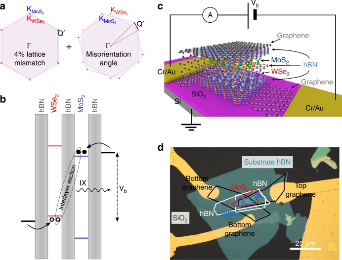
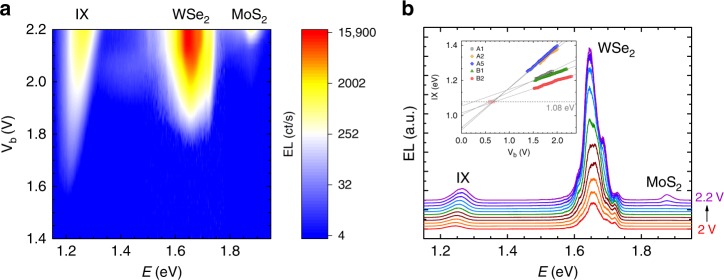
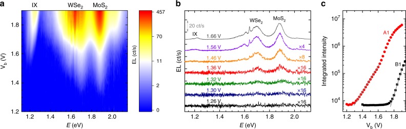
The intriguing physics of carrier-carrier interactions, which likewise affect the operation of light emitting devices, stimulate the research on semiconductor structures at high densities of excited carriers, a limit reachable at large pumping rates or in systems with long-lived electron-hole pairs. By electrically injecting carriers into WSe2/MoS2 type-II heterostructures which are indirect in real and k-space, we establish a large population of typical optically silent interlayer excitons. Here, we reveal their emission spectra and show that the emission energy is tunable by an applied electric field. When the population is further increased by suppressing the radiative recombination rate with the introduction of an hBN spacer between WSe2 and MoS2, Auger-type and exciton-exciton annihilation processes become important. These processes are traced by the observation of an up-converted emission demonstrating that excitons gaining energy in non-radiative Auger processes can be recovered and recombine radiatively.


Conflict of interest statement

The authors declare no competing interests.

Figures

Fig. 1
Fig. 1
Sample structure and selective charge carrier injection. a Brillouin zones of WSe2 (red) and MoS2 (blue) illustrating the momentum Q’ arising due to lattice mismatch and misorientation angle. b Schematic illustration of the type-II band alignment for the MoS2/WSe2 heterostructures with a middle monolayer hBN spacer. The conduction and valence band of WSe2 (MoS2) are represented by red (blue) lines. The hBN layers are represented by gray-shaded rectangles. The black lines depict the quasi Fermi levels in the bottom and top graphene electrodes for an applied voltage above the threshold for hole tunneling into WSe2 and electron tunneling into MoS2. The dashed ellipse indicates the formation of an interlayer exciton consisting of an electron in the conduction band of MoS2 and a hole in the valence band of WSe2. c Schematic drawing of the heterostructure shown in (b). d Optical microscope image of the active area of device B1
Fig. 2
Fig. 2
Interlayer excitons. a False color contour plot of the EL spectra as a function of bias voltage for sample B1 without monolayer hBN spacer. b EL spectra for biases in the range of Vb = 2.0–2.2 V extracted from (a). The spectra are vertically shifted for clarity. The inset in panel (b) shows the peak position of the IX as a function of bias for five different samples and linear fits to the dependencies. The gray dashed line marks the energy of 1.08 eV, which is an estimation for the energy of a presumptive IX without electrically injected carriers. We obtain this value by using threshold voltages of ~0.6–0.7 V (red shaded area) for measurable carrier injection extracted from photoluminescence and reflectance contrast measurements (see Supplementary Note 4)
Fig. 3
Fig. 3
Upconverted electroluminescence. a False color contour plot of the EL spectra as a function of bias voltage for sample A1 with a monolayer hBN spacer. b EL spectra for seven different bias voltages extracted from (a). The spectra are vertically shifted for clarity. For a voltage of Vb = 1.32 V emission at energies up to around 1.9 eV are observed, clearly illustrating the large upconversion effect. c Comparison of the integrated EL intensity in the spectral range of intralayer emission (1.32–2.37 eV) as a function of bias voltage for sample A1 (red circles) and B1 (black squares). A background signal from the response at Vb = 0 V was subtracted for each spectrum. The integrated EL intensity at voltages below the onset of observable emission corresponds to the noise level of our setup of around 2 ct/s per pixel (integrated over about 4000 pixels)
Fig. 4
Fig. 4
Mechanism of upconverted emission in the two-particle picture. The solid lines represent the excitonic ground-state dispersion n1 of the IX (gray), MoS2 (blue) and WSe2 (red). The circles stand for excitons. Q′ is the momentum mismatch as defined in Fig. 1a. The dashed lines indicate excited states n and the shaded area marks the excitonic continuum n. The gray-scale shading of circles schematically pictures the momentum distribution of excitons. A bright shading indicates less excitons for a given momentum than a dark shading. The photon dispersion is overlaid (gray lines) to mark the region of effective radiative recombination (orange circles). For the situation depicted, the bias voltage is below the threshold for direct intralayer charge injection. Mechanism (I) illustrates radiative IX emission facilitated by an increasing number of IX with large momenta. Mechanism (II) depicts excitonic Auger processes. The gray ellipse schematically highlights the interaction between two exemplary excitons. As a result of the interaction, one exciton recombines non-radiatively and transfers the energy to the other exciton (arrows with dotted lines). Relaxation: (i) describes relaxation back to the IX ground state (exciton–exciton annihilation), (ii) and (iii) relaxation to MoS2 and WSe2, respectively, which leads to upconverted intralayer emission

References

    1. Pandey AK, Nunzi JM. Upconversion injection in rubrene/perylene-diimide-heterostructure electroluminescent diodes. Appl. Phys. Lett. 2007;90:263508. doi: 10.1063/1.2752540. - DOI
    1. Qian L, et al. Electroluminescence from light-emitting polymer/ZnO nanoparticle heterojunctions at sub-bandgap voltages. Nano Today. 2010;5:384–389. doi: 10.1016/j.nantod.2010.08.010. - DOI
    1. He SJ, Wang DK, Jiang N, Tse JS, Lu ZH. Tunable excitonic processes at organic heterojunctions. Adv. Mater. 2016;28:649–654. doi: 10.1002/adma.201504287. - DOI - PubMed
    1. Iveland J, Martinelli L, Peretti J, Speck JS, Weisbuch C. Direct measurement of Auger electrons emitted from a semiconductor light-emitting diode under electrical injection: identification of the dominant mechanism for efficiency droop. Phys. Rev. Lett. 2013;110:177406. doi: 10.1103/PhysRevLett.110.177406. - DOI - PubMed
    1. Sun D, et al. Observation of rapid exciton–exciton annihilation in monolayer molybdenum disulfide. Nano Lett. 2014;14:5625–5629. doi: 10.1021/nl5021975. - DOI - PubMed

Publication types