. 2019 Jul;14(7):674-678.
doi: 10.1038/s41565-019-0467-1. Epub 2019 Jun 17.

Defect induced, layer-modulated magnetism in ultrathin metallic PtSe2

Affiliations

Defect induced, layer-modulated magnetism in ultrathin metallic PtSe2

Ahmet Avsar et al. Nat Nanotechnol. 2019 Jul.

Abstract

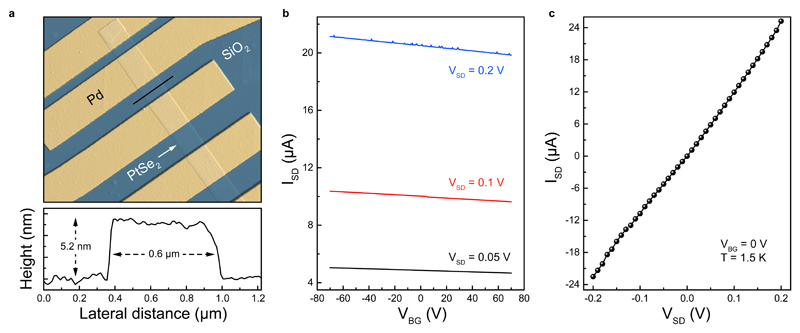
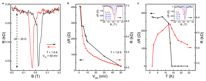
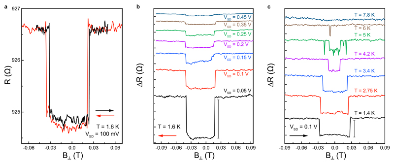
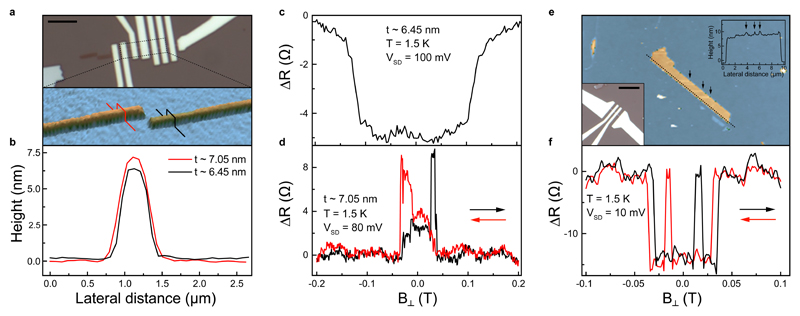
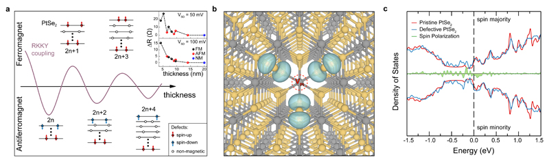
Defects are ubiquitous in solids and often introduce new properties that are absent in pristine materials. One of the opportunities offered by these crystal imperfections is an extrinsically induced long-range magnetic ordering1, a long-time subject of theoretical investigations1-3. Intrinsic, two-dimensional (2D) magnetic materials4-7 are attracting increasing attention for their unique properties, which include layer-dependent magnetism4 and electric field modulation6. Yet, to induce magnetism into otherwise non-magnetic 2D materials remains a challenge. Here we investigate magneto-transport properties of ultrathin PtSe2 crystals and demonstrate an unexpected magnetism. Our electrical measurements show the existence of either ferromagnetic or antiferromagnetic ground-state orderings that depends on the number of layers in this ultrathin material. The change in the device resistance on the application of a ~25 mT magnetic field is as high as 400 Ω with a magnetoresistance value of 5%. Our first-principles calculations suggest that surface magnetism induced by the presence of Pt vacancies and the Ruderman-Kittel-Kasuya-Yosida (RKKY) exchange couplings across ultrathin films of PtSe2 are responsible for the observed layer-dependent magnetism. Given the existence of such unavoidable growth-related vacancies in 2D materials8,9, these findings can expand the range of 2D ferromagnets into materials that would otherwise be overlooked.


Conflict of interest statement

Competing interests

The authors declare no competing interests.

Figures

Figure 1
Figure 1. Device structure and basic characterization.
a, An AFM image of the device A. Height scale bar is ± 40 nm. Following the black dashed line, we measure a height of 5.2 nm and a width of 0.6 µm for this device. b, VBG dependence of ISD measured at fixed VSD = 0.05 V, 0.1 V and 0.2 V. c, Output characteristics of the device as a function of VSD at fixed VBG = 0 V. All charge transport measurements were performed at 1.5 K.
Figure 2
Figure 2. Bias and temperature dependent magnetoresistance measurements in device A.
a, Magnetic field dependence of the device resistance measured at T = 1.6 K. The red (black) arrow represents sweep direction from 0.2 T (-0.2 T) to –0.2 T (0.2 T). b, Source-drain bias (VSD) dependences of the change in the device resistance under the magnetic field (ΔR) and the longitudinal device resistance (R). Inset shows the resistance change under magnetic field acquired at fixed biases of VSD = 1 mV, 3 mV and 50 mV. ΔR is calculated by subtracting a polynomial fitting from the device resistance (Supplementary Information 15). c, Temperature dependence of ΔR and R. Inset shows the magnetic field dependence of the resistance change measured at T = 1.5 K, 13 K and 16 K.
Figure 3
Figure 3. Bias and temperature dependent magnetoresistance measurements in device B (~ 9 nm thick).
a, Magnetic field dependence of the device resistance. The red (black) arrow represents the sweep direction from positive (negative) to negative (positive) values. b, VSD dependence of the magneto-resistance change measured at T = 1.5 K. Scale bar is 5 Ω. Curves shown for sweeps at 0.1 V ≤ VSD ≤ 0.45 V are offset for clarity. c, Temperature dependence of ΔR measured at fixed bias of VSD = 0.1 V. Scale bar is 2 Ω. Curves shown for sweeps at 2.75 K ≤ T ≤ 7.8 K are offset for clarity.
Figure 4
Figure 4. Layer-dependent magnetoresistance measurements.
a, Optical and AFM images of a completed PtSe2 device and its crystal, respectively. Dashed area represents the scanned AFM region. b. Cross-sectional plots along the red and black lines in a. AFM scans show that crystals used in device C and device D has one-layer difference (~ 0.6 nm) in their heights. c, Magnetic field dependence of ΔR measured from the device C (6.45 nm thick). d, Magnetic field dependence of ΔR measured from device D (~ 7.05 nm thick). e, AFM image of a PtSe2 crystal having multiple one-layer thick fragments on its surface. Top inset shows the cross-sectional plots along the black line in e. Black color arrows in e and top-inset e indicate the one-layer thick fragments. Bottom-inset e shows the optical image of the corresponding device. Black solid line represents the scale bar (5 µm) f, Magnetic field dependence of ΔR measured from the device E shown in e. We would like to note that the change in device resistance in these samples has opposite sign compared to the thinner devices shown in Fig. 2-a and Fig. S4-a. Such opposite switching signs were previously observed in Co and CoFe films. To determine the origin of this behavior, the effect of the number of layers, distribution of defects and their effect on magnetism need to be extensively investigated.
Figure 5
Figure 5. Theoretical investigations of PtSe2.
a, Schematic illustration showing the oscillating RKKY interaction across the PtSe2 slab and the corresponding ground-state magnetic configurations. Inset plot shows the thickness dependence of MR curves for studied samples at fixed VSD of 50 mV and 100 mV. b, Atomic structure and spin density (turquoise) around a surface VPt defect (red, dotted circle) in multilayer PtSe2. Grey (orange) balls represent Pt (Se) atoms. Isosurfaces contour is set to 0.003 e Å-3. c, Electronic density of states of multilayer PtSe2 with (blue) and without (red) a surface Pt vacancy defect. In green, the difference between spin majority and spin minority states. Fermi level is set to zero (vertical dashed line).

References

    1. Esquinazi P, Hergert W, Spemann D, Setzer A, Ernst A. Defect-induced magnetism in solids. IEEE Trans Magn. 2013;49:4668–4674.
    1. Yazyev OV, Helm L. Defect-induced magnetism in graphene. Phys Rev B. 2007;75 125408.
    1. Osorio-Guillén J, Lany S, Barabash SV, Zunger A. Magnetism without magnetic ions: percolation, exchange, and formation energies of magnetism-promoting intrinsic defects in CaO. Phys Rev Lett. 2006;96 107203. - PubMed
    1. Huang B, et al. Layer-dependent ferromagnetism in a van der Waals crystal down to the monolayer limit. Nature. 2017;546:270–273. - PubMed
    1. Gong C, et al. Discovery of intrinsic ferromagnetism in two-dimensional van der Waals crystals. Nature. 2017;546:265–269. - PubMed