. 2019 Jun 21;10(6):416.
doi: 10.3390/mi10060416.

MEMS-Based Wavelength-Selective Bolometers

Affiliations

MEMS-Based Wavelength-Selective Bolometers

Thang Duy Dao et al. Micromachines (Basel). .

Abstract

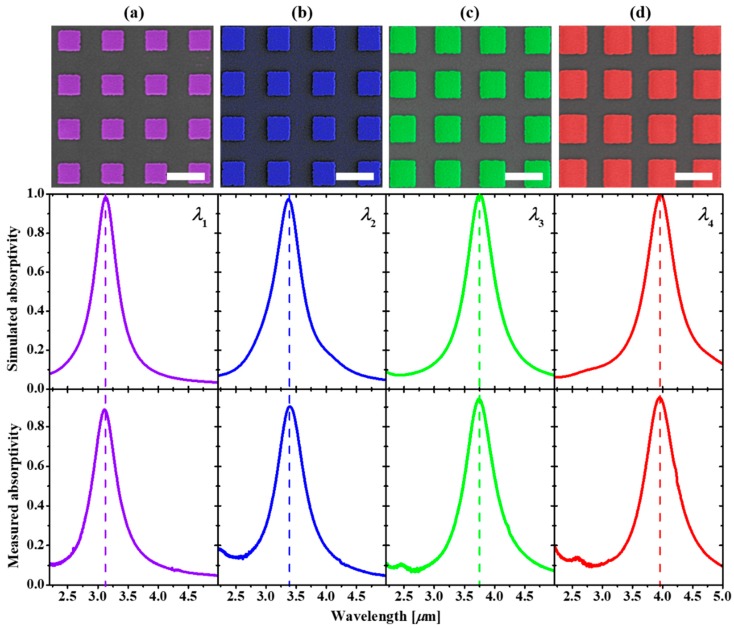
We propose and experimentally demonstrate a compact design for membrane-supported wavelength-selective infrared (IR) bolometers. The proposed bolometer device is composed of wavelength-selective absorbers functioning as the efficient spectroscopic IR light-to-heat transducers that make the amorphous silicon (a-Si) bolometers respond at the desired resonance wavelengths. The proposed devices with specific resonances are first numerically simulated to obtain the optimal geometrical parameters and then experimentally realized. The fabricated devices exhibit a wide resonance tunability in the mid-wavelength IR atmospheric window by changing the size of the resonator of the devices. The measured spectral response of the fabricated device wholly follows the pre-designed resonance, which obviously evidences that the concept of the proposed wavelength-selective IR bolometers is realizable. The results obtained in this work provide a new solution for on-chip MEMS-based wavelength-selective a-Si bolometers for practical applications in IR spectroscopic devices.

Keywords: amorphous silicon; bolometers; infrared sensors; microelectromechanical systems (MEMS); perfect absorbers; wavelength-selective sensors.


Conflict of interest statement

The authors declare no conflicts of interest.

Figures

Figure 1
Figure 1
(a) Schematic illustrations, tilted view (bottom) and cross-sectional view (top), of the proposed MEMS-based wavelength-selective bolometer. (b) Simulated reflectance, transmittance and absorptivity of a device having geometrical parameters of p = 1.2 µm, t = 0.045 µm and w = 0.72 µm exhibits a resonance at 3.73 µm with a unity absorptivity. (c) Simulated absorptivity map of the chosen absorber for the proposed device show wide resonance tunability just simply by changing the size of the resonator while keeping other parameters unchanged (p = 1.2 µm, t = 0.045 µm). (d) Simulated angle-dependent absorptivity of the absorber reveals a wide-range working angle up to 70° of the proposed devices. The peak appeared in the shorter wavelength region indicates SPP in periodic Au square array. (eh) Simulated electric field (Ex, Ez), magnetic field–Hy and absorption maps of a device excited at the resonance. In the simulations, the incident electric field propagated along the z-axis and oscillated along the x-axis. The thicknesses of the bottom Au layer and a-Si film were fixed at 0.1 µm and 0.2 µm for all simulations.
Figure 2
Figure 2
(a) XRD patterns and (b) Measured temperature-dependent resistivity curves of the as-sputtered (blue curve) and annealed at 500 °C (red curve) a-Si films. (c) Natural-log plots represented the change of resistance—ln(R/R0) and (d) TCR values versus temperature changes of the as-sputtered (blue graphs) and annealed at 500 °C (red graphs) a-Si films. (e) Natural-log plots ln(R/R0) and (f) TCR values versus temperature changes of a variety of amorphous Si-Ge alloys.
Figure 3
Figure 3
(af) Fabrication procedure of the MEMS-based wavelength-selective absorbers. (g,h) Top-view optical microscope images of the fabricated MEMS wavelength-selective bolometers with different square antenna sizes of the individual sensors. The inset in (g) reveals a photo of the MEMS-based quad-wavelength bolometer with the clear transparent Si3N4 membrane around each bolometer. (i) Top-view SEM image of the typical MEMS sensor having a resonance 3.65 µm.
Figure 4
Figure 4
Resonance tunability in the MIR atmospheric window region of the MEMS wavelength-selective bolometers. (ad) From top to bottom panels: top-view SEM images (with colors), simulated (middle) and measured (bottom) absorptivities of a quad-wavelength bolometers chip having resonances at 3.11 µm, 3.39 µm, 3.73 µm and 3.96 µm. The scale bar is 1 µm for all SEM images.
Figure 5
Figure 5
(a) Measurement setup of the spectral response of the fabricated bolometers. (b) Measured absorptivity and (c) Measured responsivity curves of a 3.73 µm resonant bolometer.

References

    1. Gabriel K., Jarvis J., Trimmer W. Small Machines, Large Opportunities: A Report on the Emerging Field of Microdynamics: Report of the Workshop on Microelectromechanical Systems Research. AT & T Bell Laboratories; Murray Hill, NJ, USA: 1988. Sponsored by the National Science Foundation.
    1. Bryzek J. Impact of MEMS technology on society. Sens. Actuators Phys. 1996;56:1–9. doi: 10.1016/0924-4247(96)01284-8. - DOI
    1. Gardner J.W., Varadan V.K. Microsensors, Mems and Smart Devices. John Wiley & Sons, Inc.; New York, NY, USA: 2001.
    1. Judy J.W. Microelectromechanical systems (MEMS): Fabrication, design and applications. Smart Mater. Struct. 2001;10:1115–1134. doi: 10.1088/0964-1726/10/6/301. - DOI
    1. Bell D.J., Lu T.J., Fleck N.A., Spearing S.M. MEMS actuators and sensors: Observations on their performance and selection for purpose. J. Micromech. Microeng. 2005;15:S153–S164. doi: 10.1088/0960-1317/15/7/022. - DOI

LinkOut - more resources