Review
. 2019 Jun 22;10(6):419.
doi: 10.3390/mi10060419.

Micro/Nano Technologies for High-Density Retinal Implant

Affiliations
Review

Micro/Nano Technologies for High-Density Retinal Implant

Qi Zeng et al. Micromachines (Basel). .

Abstract

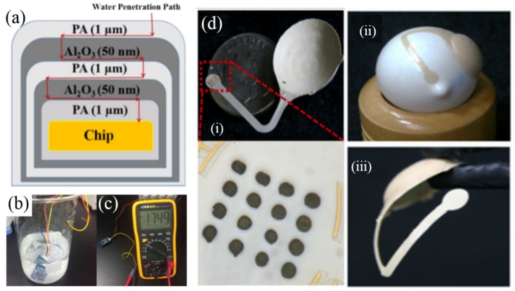
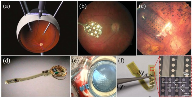
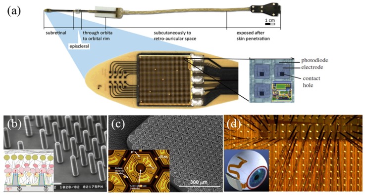
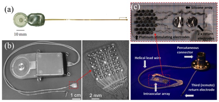
During the past decades, there have been leaps in the development of micro/nano retinal implant technologies, which is one of the emerging applications in neural interfaces to restore vision. However, higher feedthroughs within a limited space are needed for more complex electronic systems and precise neural modulations. Active implantable medical electronics are required to have good electrical and mechanical properties, such as being small, light, and biocompatible, and with low power consumption and minimal immunological reactions during long-term implantation. For this purpose, high-density implantable packaging and flexible microelectrode arrays (fMEAs) as well as high-performance coating materials for retinal stimulation are crucial to achieve high resolution. In this review, we mainly focus on the considerations of the high-feedthrough encapsulation of implantable biomedical components to prolong working life, and fMEAs for different implant sites to deliver electrical stimulation to targeted retinal neuron cells. In addition, the functional electrode materials to achieve superior stimulation efficiency are also reviewed. The existing challenge and future research directions of micro/nano technologies for retinal implant are briefly discussed at the end of the review.

Keywords: coating; high-density; implantable packaging; microelectrode array; retinal implant.


Conflict of interest statement

The authors declare no conflict of interest. The funders had no role in the design of the study; in the collection, analyses, or interpretation of data; in the writing of the manuscript, or in the decision to publish the results.

Figures

Figure 1
Figure 1
(a) External and (b) implant part of the Argus II system [7]; (c) illustration of the implantation sites of the visual cortex, epiretinal, subretinal, and supra-choroidal prostheses [7]. Reproduced with permission from [7], published by Elsevier, 2016.
Figure 2
Figure 2
(a) Illustration of the package fabrication process described by a patent from Second Sight; (b) the cross-sectional (top) and 3D illustration (bottom) of implantable body for retinal implant with 100+ channel, and (c) the major process flow for platinum/alumina composite substrate in our group.
Figure 3
Figure 3
(a) The high-density electrode array and corresponding cross-section of hermetic feedthroughs produced with four layers, Reproduced with permission from [44], published by Wiley Online Library, 2014; (b) illustration of a high-density array of diamond feedthrough and electrode with 256 channels, Reproduced with permission from [25], published by Elsevier, 2014.
Figure 4
Figure 4
Fabrication process of the base wafer: (a) Holing the substrate, (b) Au sputtering, (c) pasting dry film resist, (d) exposure and development, (e) filling Au particles and sintering, (f) film resist removal and sintering, (g) placing metal mask, (h) Au layer removal, and (i) metal mask removal. Reproduced with permission from [46], published by IOPScience, 2016.
Figure 5
Figure 5
(a) Schematic diagram of the five-layer PA/Al2O3/PA/ Al2O3/PA film on a sensor IC; (b) active soaking test for the film-coated humidity sensor at 87 °C; (c) measurement setting of the humidity sensor after active soaking test; (d) fabricated LCP-based retinal prosthesis: (i) comparison with a dime and the inner surface, and magnification of the retinal electrode array coated by iridium oxide, (ii) the device on a model eye showing conformal attachment, (iii) electrode part was precurved to fit the eye-curvature. Reproduced with permission from [55], published by IEEE, 2015.
Figure 6
Figure 6
(a) The configuration of one of the very first patient tests [57]; (b) implanted 16-channel electrode array of Argus I [7]; (c) electrode array of Argus II implant containing 60 electrodes [66]; (d) an epiretinal stimulator with a thin-film polyimide cable of gold traces [59]; (e) 126-channel electrode implanted in the eyes of mini-pigs by our group; (f) 1025-channel electrode fabricated by our group [64,65]. Reproduced from the mentioned references with permission from the related journals.
Figure 7
Figure 7
(a) The prototype of the Alpha-IMS predecessor, including 16 additional electrodes for direct stimulation. The microphotodiode array (MPDA) consists of 1500 photodiodes on a surface area of 3 × 3 mm [7]; (b) SEM of the microfabricated SU-8 pillar arrays, each pillar is about 10 μm in diameter and 40–70 μm in height. Insert: a pillar array attracts retinal cells for achieving intimate electrode-cell proximity [74]; (c) MPDA developed by the Palanker group. Insert: blown-up view of a single stimulating element with 3 photodiodes in series [7]; (d) Boston retinal implant chip, showing some of the 256 electrode current drivers. Insert: retinal implant concept with the secondary coil surrounding the cornea [73]. Reproduced from the mentioned references with permission from the related journals.
Figure 8
Figure 8
(a) A suprechoroidal implant for transretinal stimulation [70]; (b) the supra-choroidal-transretinal stimulation (STS) implant including the suprachoroidal stimulating array and the remote return electrode [77]; (c) the Bionic Vision Australia (BVA) implant with 1 remote return and 2 other return electrodes on the suprachoroidal array [15]. Reproduced from the mentioned references with permission from the related journals.
Figure 9
Figure 9
Scanning electron microscope (SEM) of different materials: (a) Pt-nanograss coating [80]; (b) cauliflower-like Pt coating [87]; (c) the fabrication process of depositing porous structure on electrode surface by templating [88]; (d) 3D nanocrystal Pt coating obtained by our group; (e) nanostructured Au coating by removing Ag from the Au–Ag alloy [96]; (f) IrOx/Pt nanocone composite coating in our group [94]; (g) IrOx/Pt nanoleaf composite coating in our group [95]. Reproduced from the mentioned references with permission from the related journals.
Figure 10
Figure 10
(a) Chemical structures of PPy and PEDOT [108]; (b) SEM image of PEDOT coating [109]; (c) SEM image of PEDOT obtained using polystyrene as template [105]; (d) SEM image of PEDOT/DCDPGYIGSR composite coating [106]; (e) Neurotrophic factor combined with PEDOT promoted the growth of neural cells [107]. Reproduced from the mentioned references with permission from the related journals.
Figure 11
Figure 11
(a) Transmission electron microscope (TEM) of multi-walled carbon nanotube (MWCNT) with amorphous carbon before and after plasma treatment [115]; (b) fluorescent images of neuron cells cultured on as-grown carbon nanotubes (CNTs) and UV-ozone-modified CNTs, and corresponding SEM images [117]; (c) Process flow of MWCNT amino-functionalization [118]; (d) the percentages of CNTs remaining after 5 min sonication vs. microwave treatment time at various powers [123]; (e) SEM image of reduced graphene oxide (GO) coating [124]; (f) SEM images of neural cells attached well to GO coating [125]; (g) histological studies of tissue response to GO coating [122]. Reproduced from the mentioned references with permission from the related journals.
Figure 12
Figure 12
(a) TEM image of IrOx-CNT composite coating [127]; (b) Cyclic voltammetry (CV) curves of bare Pt, IrOx, and IrOx-CNT coated electrodes in PBS (pH = 7.4) at sweep rate of 20 mV⋅s−1 [127]; (c) SEM image of IrOx-GO composite coating [129]; (d) SEM image of SWNT-PPy composite coating [130]; (e) Influence of peptide bond on PEDOT/PSS/MWCNT composite coating [131]. Reproduced from the mentioned references with permission from the related journals.

Similar articles

Cited by

References

    1. Schwarz D.A., Lebedev M.A., Hanson T.L., Dimitrov D.F., Lehew G., Meloy J., Rajangam S., Subramanian V., Ifft P.J., Li Z. Chronic, wireless recordings of large-scale brain activity in freely moving rhesus monkeys. Nat. Methods. 2014;11:670. doi: 10.1038/nmeth.2936. - DOI - PMC - PubMed
    1. Lee S.B., Yin M., Manns J.R., Ghovanloo M. A wideband dual-antenna receiver for wireless recording from animals behaving in large arenas. IEEE Trans. Biomed. Eng. 2013;60:1993–2004. - PMC - PubMed
    1. Yin M., Borton D.A., Komar J., Agha N., Lu Y., Li H., Laurens J., Lang Y., Li Q., Bull C. Wireless neurosensor for full-spectrum electrophysiology recordings during free behavior. Neuron. 2014;84:1170–1182. doi: 10.1016/j.neuron.2014.11.010. - DOI - PubMed
    1. Greatbatch W., Holmes C.F. History of implantable devices. IEEE Eng. Med. Biol. Mag. 1991;10:38–41. doi: 10.1109/51.84185. - DOI - PubMed
    1. Magjarević R., Ferek-Petrić B. Implantable cardiac pacemakers–50 years from the first implantation. Slov. Med. J. 2010;79:55–67.

LinkOut - more resources