. 2019 Jun 24;10(1):2774.
doi: 10.1038/s41467-019-10672-5.

High sensitivity variable-temperature infrared nanoscopy of conducting oxide interfaces

Affiliations

High sensitivity variable-temperature infrared nanoscopy of conducting oxide interfaces

Weiwei Luo et al. Nat Commun. .

Abstract

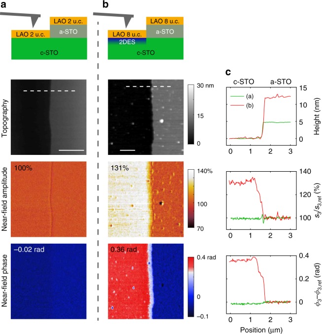
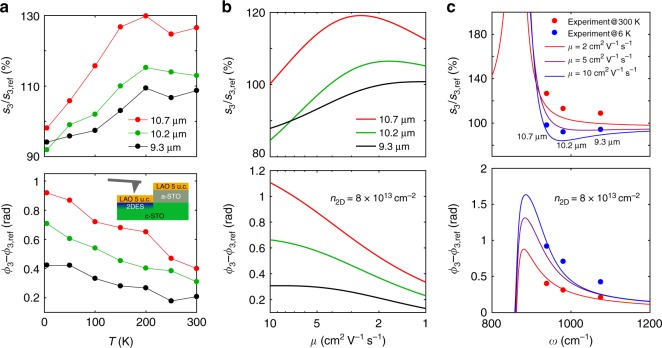
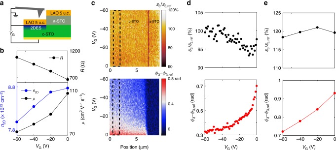
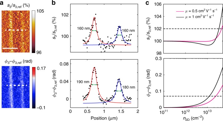
Probing the local transport properties of two-dimensional electron systems (2DES) confined at buried interfaces requires a non-invasive technique with a high spatial resolution operating in a broad temperature range. In this paper, we investigate the scattering-type scanning near field optical microscopy as a tool for studying the conducting LaAlO3/SrTiO3 interface from room temperature down to 6 K. We show that the near-field optical signal, in particular its phase component, is highly sensitive to the transport properties of the electron system present at the interface. Our modeling reveals that such sensitivity originates from the interaction of the AFM tip with coupled plasmon-phonon modes with a small penetration depth. The model allows us to quantitatively correlate changes in the optical signal with the variation of the 2DES transport properties induced by cooling and by electrostatic gating. To probe the spatial resolution of the technique, we image conducting nano-channels written in insulating heterostructures with a voltage-biased tip of an atomic force microscope.


Conflict of interest statement

The authors declare no competing interests.

Figures

Fig. 1
Fig. 1
Demonstration of the sensitivity of s-SNOM to the presence of the 2DES at room temperature. a, b Sample description and images of the AFM height, near-field amplitude and near-field phase for the two samples with different thickness of LAO (2 and 8 u.c. respectively). The conducting 2DES is present only in (b), as the LAO thickness exceeds 4 u.c. c Line profiles along the dashed lines in (a) and (b). The near-field signal s3exp(iϕ3) at the third harmonic is normalized to the signal s3,refexp(iϕ3,ref) in the reference region with an additional layer of a-STO. The laser wavelength is 10.7 μm. The scale bars are 1 μm
Fig. 2
Fig. 2
Theoretical dispersion of plasmon–phonon polaritons in the LAO/STO interface and the effect of the 2DES on the near-field response. ac Optical dispersion for 2 nm of LAO on STO without a 2DES (a), LAO/STO containing a 2DES with the optical mobility of 10 cm2 V−1 s−1 (b), and 2 cm2 V−1 s−1 (c). The 2DES confinement is modeled by an exponential distribution of the 3D density with a total 2D carrier density of 8 × 1013 cm−2 and a confinement decay of 2 nm. The dashed white curves represent the momentum dependence of time-averaged near-field coupling weight function, which peaks at qopt/2π = 2.2 × 104 cm−1. d The calculated real (top panel) and imaginary (bottom panel) parts of the reflection coefficient rp(ω) at the optimal momentum, for the three cases a, b, and c. The insets show the frequency range around 1000 cm−1. e Near-field amplitude (top panel) and phase (bottom panel) spectra normalized to a perfect metal (with rp = 1) for the three cases calculated using the point-dipole model. The green dash-dotted lines in (ac) and green regions in (d, e) show the spectral range in our experiment
Fig. 3
Fig. 3
Temperature and frequency dependence of the near-field signal on the 2DES. a Experimental temperature dependence of the near-field amplitude and phase at laser wavelengths of 9.3, 10.2, and 10.7 μm. The inset in the bottom panel shows the schematic view of the sample with 5 u.c. of LAO. b Calculated dependence of the near-field signal on the optical mobility for the same wavelengths as in (a). c Calculated frequency dependence of the near-field signals for carrier mobility of 2, 5, and 10 cm2 V−1 s−1. The experimental data at room temperature and 6 K are added for comparison. The 2D carrier density in (b, c) is 8 × 1013 cm−2
Fig. 4
Fig. 4
The effect of electrostatic gating on the electrical transport and near-field signal at 6 K. a Schematic view of the sample with a back gate. b The DC resistance, carrier density and mobility as a function of the gate voltage measured in an independent Hall-effect experiment on the same sample. c Experimental near-field amplitude and phase with respect to the reference region as a function of the position and the gate voltage. d The averaged near-field signals in the area marked by the dashed rectangles shown in c as a function of the gate voltage. e Calculation of the gate dependence of the near-field signal performed using the carrier density values and carrier mobility 20 times smaller than the DC values shown in (b). The wavelength is 10.7 μm
Fig. 5
Fig. 5
s-SNOM imaging of the AFM-written conducting wires in the LAO/STO interface with 3 u.c. of LAO. a Images of the near-field amplitude and phase, with respect to the signal from the regions not affected by the writing procedure. b The line profiles along the dashed lines in (a). c Calculated near-field signals on LAO/STO/2DES normalized by that on LAO/STO, as a function of the carrier density for optical mobility of 0.5 and 1 cm2 V−1 s−1. The dashed lines indicate the near-field amplitude and phase values of the left wire in (a). Near-field measurements are performed at room temperature, about 80 min after the AFM-writing. The laser wavelength is 10.7 μm. The scale bar is 1 μm

References

    1. Ohtomo A, Hwang H. A high-mobility electron gas at the LaAlO3/SrTiO3 heterointerface. Nature. 2004;427:423–426. doi: 10.1038/nature02308. - DOI - PubMed
    1. Thiel S, Hammerl G, Schmehl A, Schneider C, Mannhart J. Tunable quasi-two-dimensional electron gases in oxide heterostructures. Science. 2006;313:1942–1945. doi: 10.1126/science.1131091. - DOI - PubMed
    1. Zubko P, Gariglio S, Gabay M, Ghosez P, Triscone J-M. Interface physics in complex oxide heterostructures. Annu. Rev. Condens. Matter Phys. 2011;2:141–165. doi: 10.1146/annurev-conmatphys-062910-140445. - DOI
    1. Li L, et al. Very large capacitance enhancement in a two-dimensional electron system. Science. 2011;332:825–828. doi: 10.1126/science.1204168. - DOI - PubMed
    1. Reyren N, et al. Superconducting interfaces between insulating oxides. Science. 2007;317:1196–1199. doi: 10.1126/science.1146006. - DOI - PubMed

Publication types