. 2019 Jul 5;9(1):9774.
doi: 10.1038/s41598-019-46199-4.

Chemical Vapor Deposition of Organic-Inorganic Bismuth-Based Perovskite Films for Solar Cell Application

Affiliations

Chemical Vapor Deposition of Organic-Inorganic Bismuth-Based Perovskite Films for Solar Cell Application

S Sanders et al. Sci Rep. .

Abstract

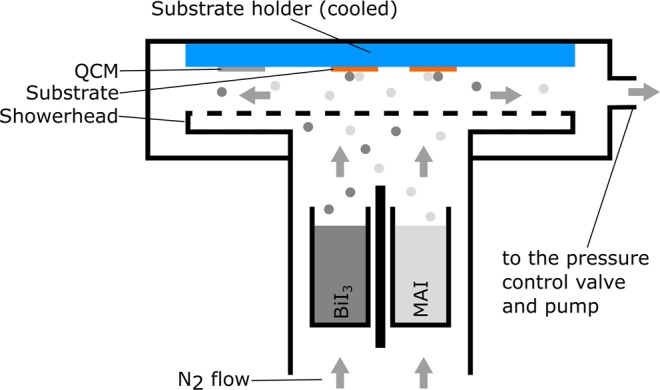
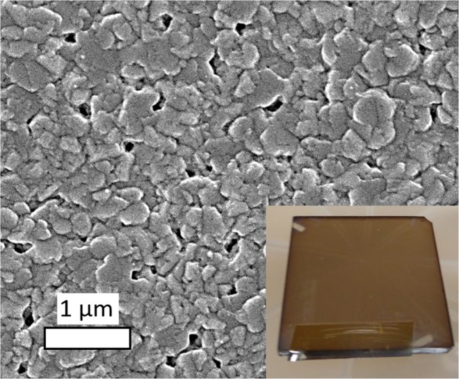
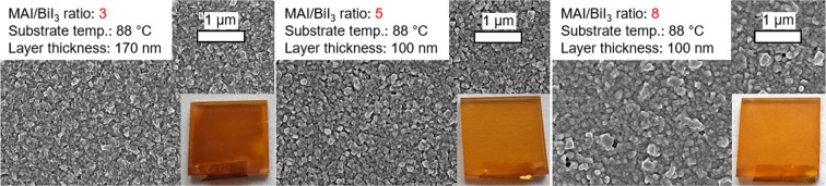
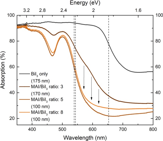
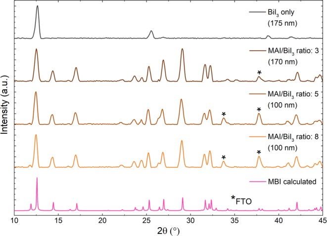
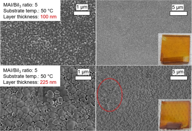
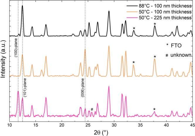
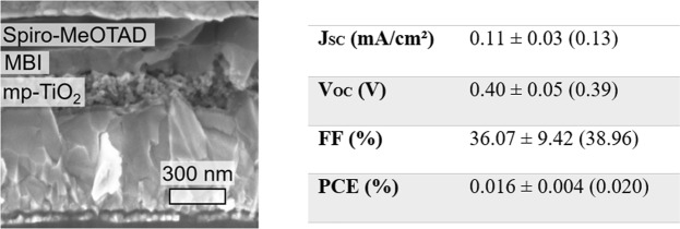
Perovskite solar cells have shown a rapid increase of performance and overcome the threshold of 20% power conversion efficiency (PCE). The main issues hampering commercialization are the lack of deposition methods for large areas, missing long-term device stability and the toxicity of the commonly used Pb-based compounds. In this work, we present a novel chemical vapor deposition (CVD) process for Pb-free air-stable methylammonium bismuth iodide (MBI) layers, which enables large-area production employing close-coupled showerhead technology. We demonstrate the influence of precursor rates on the layer morphology as well as on the optical and crystallographic properties. The impact of substrate temperature and layer thickness on the morphology of MBI crystallites is discussed. We obtain smooth layers with lateral crystallite sizes up to 500 nm. Moreover, the application of CVD-processed MBI layers in non-inverted perovskite solar cells is presented.


Conflict of interest statement

The authors declare no competing interests.

Figures

Figure 1
Figure 1
Schematic illustration of the deposition tool. The N2 flow was set to 500 sccm and the base pressure to 10 hPa.
Figure 2
Figure 2
SEM image of a pure BiI3 film (layer thickness 175 nm, temperature of the substrate 88 °C, BiI3 rate 1.0 nm/min) on FTO/c-TiO2/mp-TiO2 substrates. The inset shows the macroscopic appearance (photography, 2.5 cm × 2.5 cm).
Figure 3
Figure 3
SEM images of MBI films deposited at 88 °C substrate temperature, a BiI3 rate of 0.5 nm/min and different MAI/BiI3 rate ratios of 3, 5 and 8. The insets show the macroscopic appearances (photography, 2.5 cm × 2.5 cm).
Figure 4
Figure 4
Absorption spectra of the BiI3-only film and MBI layers on FTO/c-TiO2/mp-TiO2 substrates deposited with a BiI3 rate of 0.5 nm/min, a substrate temperature of 88 °C and different MAI/BiI3 ratios. The interpolated absorption edges are exhibited by the dashed vertical lines. The arrows illustrate the drop of absorption in the region of 500 to 650 nm for MBI layers without residual BiI3.
Figure 5
Figure 5
Calculated XRD pattern of MBI and XRD measurements of BiI3-only film and MBI layers deposited with different MAI/BiI3 ratios (3, 5 and 8), substrate temperature of 88 °C and a BiI3 rate of 0.5 nm/min.
Figure 6
Figure 6
SEM images of MBI films deposited at 50 °C substrate and layer thicknesses of 100 nm and 225 nm. The insets show the macroscopic appearances (photography, 2.5 cm × 2.5 cm).
Figure 7
Figure 7
XRD patterns of MBI grown at 50 °C substrate temperature with different layer thicknesses of 100 nm and 225 nm compared to MBI film deposited at 88 °C with 100 nm layer thickness.
Figure 8
Figure 8
SEM cross-section image (left) and PV characteristics (AM1.5, 100 mW/cm²) of MBI perovskite solar cell (right), fabricated using MBI layer deposited by CVD (50 °C substrate temperature, MAI/BiI3 ratio of 5 and 225 nm layer thickness). Average and standard deviation based on 5 devices. Characteristics of the best performing solar cell are shown in parentheses.

References

    1. Wehrenfennig C, Eperon GE, Johnston MB, Snaith HJ, Herz LM. High Charge Carrier Mobilities and Lifetimes in Organolead Trihalide Perovskites. Adv. Mater. 2014;26:1584–1589. doi: 10.1002/adma.201305172. - DOI - PMC - PubMed
    1. Shi D, et al. Solar cells. Low trap-state density and long carrier diffusion in organolead trihalide perovskite single crystals. Science. 2015;347:519–522. doi: 10.1126/science.aaa2725. - DOI - PubMed
    1. Park N-G. Perovskite solar cells. An emerging photovoltaic technology. Mater. Today. 2015;18:65–72. doi: 10.1016/j.mattod.2014.07.007. - DOI
    1. Jiang Qi, Zhao Yang, Zhang Xingwang, Yang Xiaolei, Chen Yong, Chu Zema, Ye Qiufeng, Li Xingxing, Yin Zhigang, You Jingbi. Surface passivation of perovskite film for efficient solar cells. Nature Photonics. 2019;13(7):460–466. doi: 10.1038/s41566-019-0398-2. - DOI
    1. Yang WS, et al. Iodide management in formamidinium-lead-halide-based perovskite layers for efficient solar cells. Science. 2017;356:1376–1379. doi: 10.1126/science.aan2301. - DOI - PubMed