

Electrical Properties of Double-Sided Polymer Surface Nanostructures
- PMID: 31297675
- PMCID: PMC6624224
- DOI: 10.1186/s11671-019-3071-2
Electrical Properties of Double-Sided Polymer Surface Nanostructures
Abstract
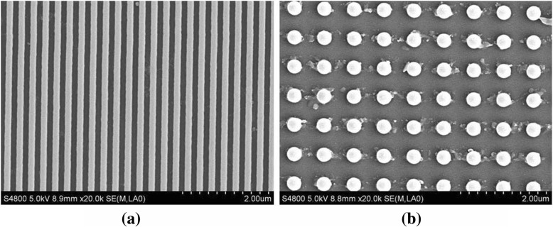
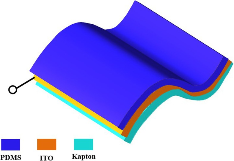
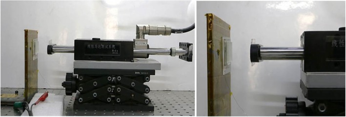
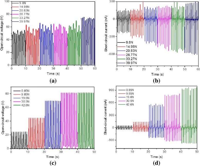
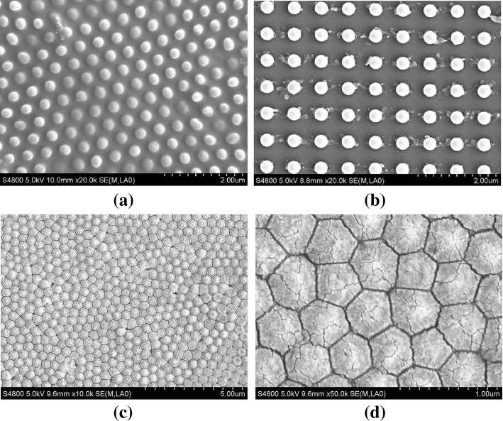
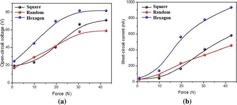
In this study, double-sided polymer surface nanostructures are fabricated using twice nanoimprint lithography and metal deposition technique. We perform electrical property measurement on these double-sided surface nanostructures. Open-circuit voltage and short-circuit current of the as-prepared samples with double-sided surface nanostructures and conductive electrode are recorded using an oscilloscope with applying different external force. The measurements are carried out at room temperature. We find that the intensity of open-circuit voltage and short-circuit current for the double-sided surface nanostructures depends strongly on the sizes, shapes, and arrangements of nanostructures and pressure force. The strongest electrical property can be observed in the hexagon nanopillar arrays with the diameter of about 400 nm containing sub-50-nm resolution sharp structures at the force of about 40 N. We discuss the physical mechanisms responsible for these interesting research findings. The experimental results we study are relevant to the applications of double-sided surface nanostructures such as a nanogenerator, pressure sensors, and nano-optoelectronic devices.
Keywords: Double-sided nanostructures; Electrical properties; Nanoimprint lithography; Open-circuit voltage; Pressure force; Short-circuit current.
Conflict of interest statement
The authors declare that they have no competing interests.
Figures
References
-
- Cavas M. Alahmed Z A, Albrithen H A, Yakuphanouglu F: Photoresponse and electrical properties of Al/nanostructure NiFe 2 O 4 /p-Si/Al photodiode. J Electroceram. 2014;32(2-3):163. doi: 10.1007/s10832-013-9862-4. - DOI
Grants and funding
LinkOut - more resources
Full Text Sources
