. 2019 Jul 30;116(31):15398-15406.
doi: 10.1073/pnas.1907697116. Epub 2019 Jul 15.

Flexible electronic/optoelectronic microsystems with scalable designs for chronic biointegration

Affiliations

Flexible electronic/optoelectronic microsystems with scalable designs for chronic biointegration

Enming Song et al. Proc Natl Acad Sci U S A. .

Abstract

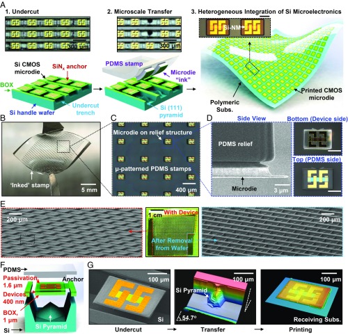
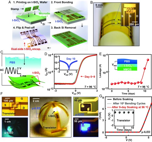
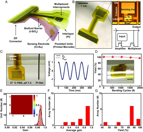
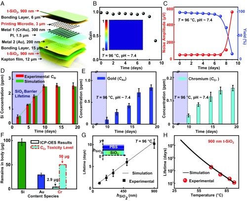
Flexible biocompatible electronic systems that leverage key materials and manufacturing techniques associated with the consumer electronics industry have potential for broad applications in biomedicine and biological research. This study reports scalable approaches to technologies of this type, where thin microscale device components integrate onto flexible polymer substrates in interconnected arrays to provide multimodal, high performance operational capabilities as intimately coupled biointerfaces. Specificially, the material options and engineering schemes summarized here serve as foundations for diverse, heterogeneously integrated systems. Scaled examples incorporate >32,000 silicon microdie and inorganic microscale light-emitting diodes derived from wafer sources distributed at variable pitch spacings and fill factors across large areas on polymer films, at full organ-scale dimensions such as human brain, over ∼150 cm2 In vitro studies and accelerated testing in simulated biofluids, together with theoretical simulations of underlying processes, yield quantitative insights into the key materials aspects. The results suggest an ability of these systems to operate in a biologically safe, stable fashion with projected lifetimes of several decades without leakage currents or reductions in performance. The versatility of these combined concepts suggests applicability to many classes of biointegrated semiconductor devices.

Keywords: bioelectronics; biomedical implants; electrocorticography; flexible electronics; heterogeneous integration.


Conflict of interest statement

The authors declare no conflict of interest.

Figures

Fig. 1.
Fig. 1.
Scalable approaches for deterministic assembly of semiconductor microdevices into flexible systems for biointegration. (A) Processing schemes for printing of flexible silicon microdie: 1) Formation of trenches on a wafer substrate; 2) retrieval with a PDMS stamp; and 3) printing on a polymeric substrate. Insets are optical images of arrays of microdie on a source wafer before/after transfer, and silicon microdie printed onto a receiving substrate (scale bar, 100 μm). (B) Photographs of a PMDS stamp inked with ∼1,000 microdie. (C) Magnified image of an array of microdie on a PDMS stamp. (D) SEM and optical images of an inked PDMS stamp in side, bottom, and top views (scale bar, 100 μm). (E, Left) SEM image of a large array of microdie released from the source wafer after undercut etching. (E, Middle) Photograph of an entire source wafer. Red and blue frames correspond to areas with and without released arrays of microdie, respectively. (E, Right) SEM image of an etched structure after complete removal of an array of microdie. (F) Schematic illustration of the material stack layout and thicknesses of the different layers at the location of a microdie after complete release. (G) A group of SEM and optical profilometry images shown in sequence for a representative unit cell after undercut, after removal and after priniting onto a target substrate. The undercut angle in the silicon is 54.7°, consistent with the anisotropic behavior of the etchant.
Fig. 2.
Fig. 2.
Microtransfer printing of microdie at different densities. (A) Schematic illustration for printing in the geometry of an N: 1) Preparation of a PDMS stamp for deterministic assembly by transfer printing. Insets are optical images of PDMS stamps with sparse/dense distributions of relief features, where W and L are the width and length of the space between pixels; 2) printing on a flexible substrate in the geometry of an N pattern. (B and C) Photographs of a large collection of microdie (total ∼32,000) printed on a large polymer film cut into the approximate outline of a human brain, while flat (B) and bent (C). B, Insets, are optical images (Upper) of the printed array at different densities, with magnified images; Mid and Lower Insets are of sparse (blue frame) and dense regions (black frame), respectively. C, Inset, is printing yield as function of printing number. (D) Schematic illustration of contact of the system on the surface of a brain model. Dense arrays align to areas of primary sensory cortex. (E) SEM image of a microdie array integrated with sensing electrodes (Au, 300 nm). Inset shows the subsequent metal interconnect. (F) Statistics of the peak effective mobility (μeff), VT, and the on/off ratio of 300 printed transistors.
Fig. 3.
Fig. 3.
Integration of electronic/optoelectronic microsystems with thin biofluid barriers of t-SiO2. (A) Schemes for encapsulating systems with t-SiO2. (B) Optical image of a 2 × 2 transistor array with t-SiO2 on both sides. Inset shows a single mircodie covered by t-SiO2. (C) Schematic diagram of a system immersed in PBS solution while under electrical bias. (D and E) Accelerated soak test results for a single printed microdie with transfer characteristics (D) and leakage currents (E) collected during immersion in PBS solution at 96 °C and pH 7.4. Insets show the point of catastrophic failure after a stable lifetime and schematic illustrations of the soak test, repectively. The applied voltage (Vapp) for the leakage analysis is d.c. 3 V. (F and G) Printed cointegration of optoelectronic and electronic components into a system encapsulated by t-SiO2 layers. (F) Photograph of printed μ-ILEDs and microdie in a starburst-shaped system wrapped over a table-tennis ball. Insets are optical images of a transistor and an μ-ILED in off and on states. (G) Bending tests and accelerated soak tests of a system with printed μ-ILEDs and transistors. Inset shows transistor performance.
Fig. 4.
Fig. 4.
Systems of printed assemblies of microdie with multiplexing capabilities for electrophysiological mapping. (A) An exploded-view schematic illustration of the key functional layers and (B) a photograph of a flexible sensing system with 128 silicon transistors in a slightly bent state. Zero insertion force (ZIF) connectors provide interfaces to external electronics for data acquisition. Insets in B are an optical microscope image (Upper, scale bar of 80 μm) and a circuit diagram (Lower) of a cell unit. (C, Left) An image of a device completely immersed in 37 °C PBS solution, pH 7.4. (C, Right) Output response of a unit cell with respect to an input sine wave (2 mV, 10 Hz). (D) Yield as a function of cycles of bending to a radius of curvature of 1 cm. Inset is an optical image of a system under bending. (Scale bar, 5 mm.) (E) Histogram (with Gaussian lineshape fitting) of gain values from 64 channels of a typical system. The results indicate 100% yield and near-unity average gain. Inset is a spatial map of gain values. (F and G) Cumulative statistics of average gain and yield of 10 different array of this type.
Fig. 5.
Fig. 5.
Chronic stability and biocompatibility assessments. (A) Exploded-view schematic illustration of the layer configuration for an 8 × 8 array of printed microdie for multiplexed adressing. (B and C) In vitro results of an active system during soak tests at 96 °C, including gain, noise amplitude, and yield. Inset is a map of gain after 10-d soaking in 96 °C PBS. (D and E) ICP-OES results. (D) Si concentration in the PBS used for the accelerated tests. The simulated (green) and measured (red) results show a linear relationship with a rate of ∼0.27 ppm/d, followed by saturation after dissolution of the t-SiO2 layer. (E) Metal concentration in PBS. Electrode materials such as Au (Left) and Cr (Right) start to release in PBS solution (from day 10) after dissolution of the t-SiO2. (F) Biocompatibility assessment of the active microdie array. (G) Thickness-dependent and (H) temperature-dependent lifetimes of a t-SiO2 barrier with simulated (line) and measured (symbols) results. Inset in G is the schematic illustration.

Similar articles

Cited by

  • Technology Roadmap for Flexible Sensors.
    Luo Y, Abidian MR, Ahn JH, Akinwande D, Andrews AM, Antonietti M, Bao Z, Berggren M, Berkey CA, Bettinger CJ, Chen J, Chen P, Cheng W, Cheng X, Choi SJ, Chortos A, Dagdeviren C, Dauskardt RH, Di CA, Dickey MD, Duan X, Facchetti A, Fan Z, Fang Y, Feng J, Feng X, Gao H, Gao W, Gong X, Guo CF, Guo X, Hartel MC, He Z, Ho JS, Hu Y, Huang Q, Huang Y, Huo F, Hussain MM, Javey A, Jeong U, Jiang C, Jiang X, Kang J, Karnaushenko D, Khademhosseini A, Kim DH, Kim ID, Kireev D, Kong L, Lee C, Lee NE, Lee PS, Lee TW, Li F, Li J, Liang C, Lim CT, Lin Y, Lipomi DJ, Liu J, Liu K, Liu N, Liu R, Liu Y, Liu Y, Liu Z, Liu Z, Loh XJ, Lu N, Lv Z, Magdassi S, Malliaras GG, Matsuhisa N, Nathan A, Niu S, Pan J, Pang C, Pei Q, Peng H, Qi D, Ren H, Rogers JA, Rowe A, Schmidt OG, Sekitani T, Seo DG, Shen G, Sheng X, Shi Q, Someya T, Song Y, Stavrinidou E, Su M, Sun X, Takei K, Tao XM, Tee BCK, Thean AV, Trung TQ, Wan C, Wang H, Wang J, Wang M, Wang S, Wang T, Wang ZL, Weiss PS, Wen H, Xu S, Xu T, Yan H, Yan X, Yang H, Yang L, Yang S, Yin L, Yu C, Yu G, Yu J, Yu SH, Yu X, Zamburg E, Zhang H, Zhang X, Zhang X, Zhang X, Zhang Y, Zhang Y, Zhao S, Zhao X, Zheng Y, Zheng YQ, Zheng Z, Zhou T, Zhu B, Zhu M, Zhu R, Zh… See abstract for full author list ➔ Luo Y, et al. ACS Nano. 2023 Mar 28;17(6):5211-5295. doi: 10.1021/acsnano.2c12606. Epub 2023 Mar 9. ACS Nano. 2023. PMID: 36892156 Free PMC article. Review.
  • Transient charge-driven 3D conformal printing via pulsed-plasma impingement.
    Jiang Y, Ye D, Li A, Zhang B, Han W, Niu X, Zeng M, Guo L, Zhang G, Yin Z, Huang Y. Jiang Y, et al. Proc Natl Acad Sci U S A. 2024 May 28;121(22):e2402135121. doi: 10.1073/pnas.2402135121. Epub 2024 May 21. Proc Natl Acad Sci U S A. 2024. PMID: 38771869 Free PMC article.
  • A biomaterial-silicon junction for photodetection.
    Gogurla N, Wahab A, Kim S. Gogurla N, et al. Mater Today Bio. 2023 Apr 24;20:100642. doi: 10.1016/j.mtbio.2023.100642. eCollection 2023 Jun. Mater Today Bio. 2023. PMID: 37153757 Free PMC article.
  • Tracking neural activity from the same cells during the entire adult life of mice.
    Zhao S, Tang X, Tian W, Partarrieu S, Liu R, Shen H, Lee J, Guo S, Lin Z, Liu J. Zhao S, et al. Nat Neurosci. 2023 Apr;26(4):696-710. doi: 10.1038/s41593-023-01267-x. Epub 2023 Feb 20. Nat Neurosci. 2023. PMID: 36804648
  • Shape-changing electrode array for minimally invasive large-scale intracranial brain activity mapping.
    Wei S, Jiang A, Sun H, Zhu J, Jia S, Liu X, Xu Z, Zhang J, Shang Y, Fu X, Li G, Wang P, Xia Z, Jiang T, Cao A, Duan X. Wei S, et al. Nat Commun. 2024 Jan 24;15(1):715. doi: 10.1038/s41467-024-44805-2. Nat Commun. 2024. PMID: 38267440 Free PMC article.

References

    1. Jun J. J., et al. , Fully integrated silicon probes for high-density recording of neural activity. Nature 551, 232–236 (2017). - PMC - PubMed
    1. Jeong J.-W., et al. , Wireless optofluidic systems for programmable in vivo pharmacology and optogenetics. Cell 162, 662–674 (2015). - PMC - PubMed
    1. Won S. M., et al. , Recent advances in materials, devices, and systems for neural interfaces. Adv. Mater. 30, 1800534 (2018). - PubMed
    1. Kim D.-H., et al. , Electronic sensor and actuator webs for large-area complex geometry cardiac mapping and therapy. Proc. Natl. Acad. Sci. U.S.A. 109, 19910–19915 (2012). - PMC - PubMed
    1. Fu T.-M., Hong G., Viveros R. D., Zhou T., Lieber C. M., Highly scalable multichannel mesh electronics for stable chronic brain electrophysiology. Proc. Natl. Acad. Sci. U.S.A. 114, E10046–E10055 (2017). - PMC - PubMed

Publication types

LinkOut - more resources