. 2019 Jul 17;10(1):3156.
doi: 10.1038/s41467-019-11145-5.

Chip-scale atomic diffractive optical elements

Affiliations

Chip-scale atomic diffractive optical elements

Liron Stern et al. Nat Commun. .

Erratum in

Abstract

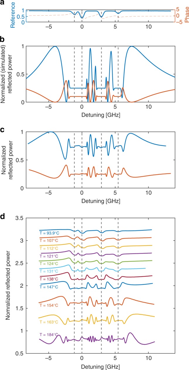
The efficient light-matter interaction and discrete level structure of atomic vapors made possible numerous seminal scientific achievements including time-keeping, extreme non-linear interactions, and strong coupling to electric and magnetic fields in quantum sensors. As such, atomic systems can be regarded as a highly resourceful quantum material platform. Recently, the field of thin optical elements with miniscule features has been extensively studied demonstrating an unprecedented ability to control photonic degrees of freedom. Hybridization of atoms with such thin optical devices may offer a material system enhancing the functionality of traditional vapor cells. Here, we demonstrate chip-scale, quantum diffractive optical elements which map atomic states to the spatial distribution of diffracted light. Two foundational diffractive elements, lamellar gratings and Fresnel lenses, are hybridized with atomic vapors demonstrating exceptionally strong frequency-dependent, non-linear and magneto-optic behaviors. Providing the design tools for chip-scale atomic diffractive optical elements develops a path for compact thin quantum-optical elements.


Conflict of interest statement

The authors declare no competing interests.

Figures

Fig. 1
Fig. 1
Atomic diffraction optical elements concept of operation. a Artistic rendition of a diffractive atomic grating whose diffraction pattern is controlled by the atomic state of atoms embedded within its channels. At the far-field plane, two different diffractive patterns are depicted corresponding to two different detuning from the optical transition (illustrated in the green circle). b Artistic rendition of an atomic switchable Fresnel lens. In the focal plane, two states of operation are shown, which correspond to two different detuning’s from the atomic state: the red state corresponds to the lens in the on-state, and the green to the off-state. c A photograph of an ADOE consisting of a rubidium reservoir connected to a few manifestations of Fresnel lens. d A photograph of three typical diced devices compared to a penny
Fig. 2
Fig. 2
Atomic diffraction grating spectroscopy. a Reference D2 rubidium absorption and calculated phase spectrum. The 0 GHz detuning is in reference to the 85Rb F = 3 state, and the phase plot is in units of 2π. b, c Spectra of zero-order (blue) and first-order (orange) atomic diffraction grating, measured by combining a photodetector and a pinhole in the far-field (b) calculated (c) measured spectra (d) evolution of the measured first-order spectra as a function of atomic density, demonstrating the evolving of the spectra from being absorptive to dispersive
Fig. 3
Fig. 3
Atomic Fresnel lens spectroscopy and characterization. a Fresnel lens spectrum at the focal point, obtained by post processing a set of recorded CCD images while simultaneously scanning the lasers frequency. Inset images are examples of such images at different frequency detunings. An additional inset shows a zoomed photograph of the actual device. b A series of CCD images recorded at the focal plane corresponding to the maximal position with detuning of −3.4 GHz to the minimal point with detuning of −2.4 GHz. c, d The spatial dependence of the focal point cross-section as function of the propagation axis plotted for the two extreme (c) on and (d) off states. Scale bar refers to figures bd and is in units of normalized reflected power
Fig. 4
Fig. 4
ADOE response as function of laser power and external magnetic field. a Normalized first-order reflected power as a function of frequency detuning of an atomic diffractive grating, with incident power of 10 mW (blue line) and 10 µW (red line). A portion of the spectra corresponding to spectroscopic data between the two absorption lines of 85Rb is shown here. b Normalized first-order reflected power as a function of frequency detuning of an atomic diffractive grating for the case where a ~300 gauss magnetic field is applied to the grating (blue lines) and in the absence of such field (red line)

References

    1. O’Shea, D. C., Suleski, T. J., Kathman, A. D., Prather, D. W. & Society of photo-optical instrumentation engineers. Diffractive Optics: Design, Fabrication, and Test (SPIE—The International Society for Optical Engineering, Bellingham, Washington, 2004).
    1. Yu N, Capasso F. Flat optics with designer metasurfaces. Nat. Mater. 2014;13:139–150. doi: 10.1038/nmat3839. - DOI - PubMed
    1. Zheludev NI, Kivshar YS. From metamaterials to metadevices. Nat. Mater. 2012;11:917–924. doi: 10.1038/nmat3431. - DOI - PubMed
    1. Segal N, Keren-Zur S, Hendler N, Ellenbogen T. Controlling light with metamaterial-based nonlinear photonic crystals. Nat. Photonics. 2015;9:180–184. doi: 10.1038/nphoton.2015.17. - DOI
    1. Chen H-T, Taylor AJ, Yu N. A review of metasurfaces: physics and applications. Rep. Prog. Phys. 2016;79:076401. doi: 10.1088/0034-4885/79/7/076401. - DOI - PubMed