. 2019 Jul 18;10(1):3161.
doi: 10.1038/s41467-019-11187-9.

Self-selective van der Waals heterostructures for large scale memory array

Affiliations

Self-selective van der Waals heterostructures for large scale memory array

Linfeng Sun et al. Nat Commun. .

Abstract

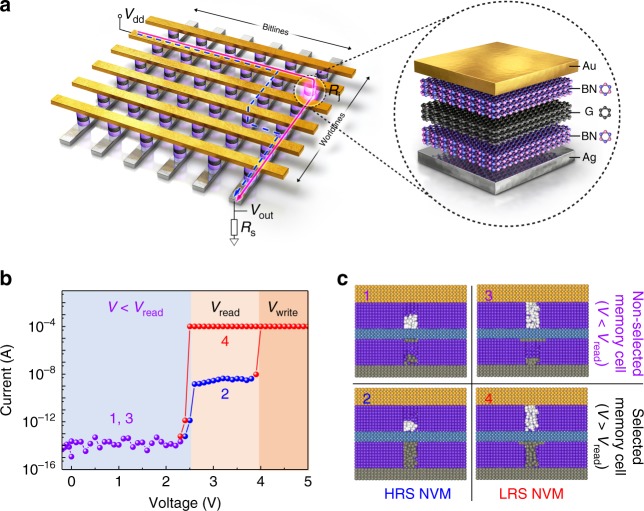
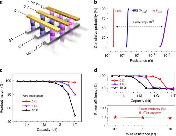
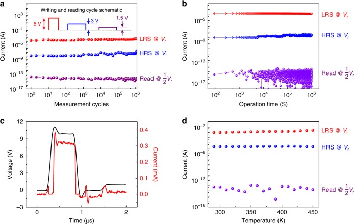
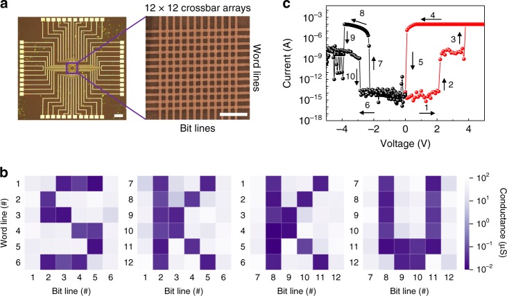
The large-scale crossbar array is a promising architecture for hardware-amenable energy efficient three-dimensional memory and neuromorphic computing systems. While accessing a memory cell with negligible sneak currents remains a fundamental issue in the crossbar array architecture, up-to-date memory cells for large-scale crossbar arrays suffer from process and device integration (one selector one resistor) or destructive read operation (complementary resistive switching). Here, we introduce a self-selective memory cell based on hexagonal boron nitride and graphene in a vertical heterostructure. Combining non-volatile and volatile memory operations in the two hexagonal boron nitride layers, we demonstrate a self-selectivity of 1010 with an on/off resistance ratio larger than 103. The graphene layer efficiently blocks the diffusion of volatile silver filaments to integrate the volatile and non-volatile kinetics in a novel way. Our self-selective memory minimizes sneak currents on large-scale memory operation, thereby achieving a practical readout margin for terabit-scale and energy-efficient memory integration.


Conflict of interest statement

The authors declare no competing interests.

Figures

Fig. 1
Fig. 1
Crossbar memory array of a self-selective van der Waals heterostructure and the working mechanism. a Schematic picture of the van der Waals heterostructure in the crossbar memory array architecture, differing from the traditional one-selector one-resistor and complementary resistive switching (see in the main text). b Current–voltage characteristics of a single memory cell. The four current and voltage ranges represent four different states of the memory cell. The selectivity of the self-selective cell is 1010, with a big memory window (103). Our unit cell shows bipolar behavior. For the negative voltage direction, it is shown in Supplementary Fig. 7a. During the measurement, the top electrode (gold) was kept to connect the ground. c Schematic illustration of hexagonal boron nitride/graphene/hexagonal boron nitride layers for the four states in ‘b’. Ranges “1” and “3” represent the high-resistance state and low-resistance state of unselected cells, respectively. Ranges “2” and “4” represent the high-resistance state and low-resistance state of a selected memory cell, respectively. Conductive silver filaments are formed at a voltage of 2.6 V, enabling the read of the high-resistance state (range “2”) and low-resistance state (range “4”) in a voltage window from 2.6 to 4.0 V. The gray, purple, blue, and yellow spheres represent silver, hexagonal boron nitride, graphene, and gold layer, respectively. The white spheres in the top hexagonal boron nitride layer represent the boron vacancies in hexagonal boron nitride
Fig. 2
Fig. 2
Memory integration of self-selective memory cells. a Schematic picture of a reading process using a one-half voltage scheme. The selected memory cell with a net voltage application of ‘V’ is highlighted in pink, while either one-half ‘V’ or zero voltage bias is applied to the other memory cells. b Reliability of the three states: the low-resistance state (probed by Vread), high-resistance state (probed by Vread), and unselected state (probed by one-half Vread) exhibit narrow voltage windows and a high selectivity of larger than 1010 in the cumulative probability of resistances. c Readout margin for three different wire resistances between neighboring cells simulated by using SPICE modeling. A 1/2 V voltage scheme was used in the simulation, while a 1/3 V voltage scheme showed a similar result (Supplementary Fig. 11). d Simulated capacity-dependent energy efficiency with three different wire resistances. An energy efficiency of 10% was observed at an integration capacity of one terabit by SPICE modeling, which is consistent with the greatly suppressed sneak current due to the high selectivity of larger than 1010 in (b). The unit wire resistance calculated in our work is less than 10 Ω (see Methods). Thus, the maximum wire resistance used for this simulation is 10 Ω
Fig. 3
Fig. 3
Stability and switching speed of our self-selective memory. a Endurance of switching behavior among the three states by a voltage pulse train over 106 measurement cycles. The resistance states were read by a wide pulse width to avoid the net charge (See Methods). b Retention behavior of the three states for a time of 106 s. c Switching speed during programming operation shows a time constant of tens of nanoseconds. A voltage pulse of 10 V for 500 ns was used for the measurement. d Stability of the three states (low-resistance state, high-resistance state, and unselected state) over temperatures ranging from 290 to 450 K, due to the high crystal quality of hexagonal boron nitride and graphene
Fig. 4
Fig. 4
Programming a code using a crossbar array with our self-selective memory cells. a Optical and scanning electron microscopy images of a 12 × 12 crossbar memory array with our self-selective van der Waals heterostructure experimentally. Scale bars: 200 and 5 μm for the optical and SEM images, respectively. b The color map of the readout conductance with a reading voltage of 3 V (one-half voltage scheme). The heavy violet color indicates a lower readout conductance, as shown in the conductance scale. c A full-voltage-range resistive switching curve of a self-selective cell fabricated on flexible PET substrate. The sequential numbers and arrows exhibit typical write and erase processes, maintaining the negligible sneak current for unselected memory cells

References

    1. Shulaker MM, et al. Three-dimensional integration of nanotechnologies for computing and data storage on a single chip. Nature. 2017;547:74. doi: 10.1038/nature22994. - DOI - PubMed
    1. Wright, E. P. G. Electric connecting device. US2667542A (1954).
    1. Kim T-W, et al. All-organic photopatterned one diode-one resistor cell array for advanced organic nonvolatile memory applications. Adv. Mater. 2012;24:827–827. doi: 10.1002/adma.201290024. - DOI - PubMed
    1. Ji Y, et al. Flexible and twistable non-volatile memory cell array with all-organic one diode–one resistor architecture. Nat. Commun. 2013;4:2707. doi: 10.1038/ncomms3707. - DOI - PubMed
    1. Kim KM, et al. Low-power, self-rectifying, and forming-free memristor with an asymmetric programing voltage for a high-density crossbar application. Nano Lett. 2016;16:6724–6732. doi: 10.1021/acs.nanolett.6b01781. - DOI - PubMed

Grants and funding

LinkOut - more resources