. 2019 Jul 18;9(1):10433.
doi: 10.1038/s41598-019-46860-y.

Optical analysis of light-emitting electrochemical cells

Affiliations

Optical analysis of light-emitting electrochemical cells

E Mattias Lindh et al. Sci Rep. .

Abstract

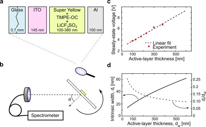
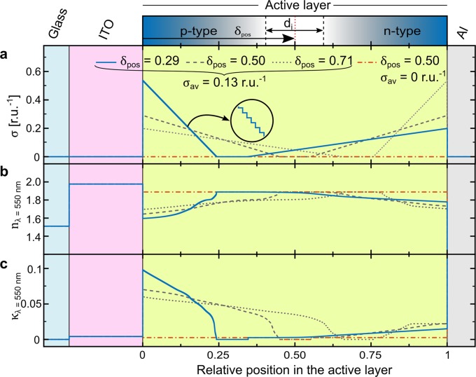
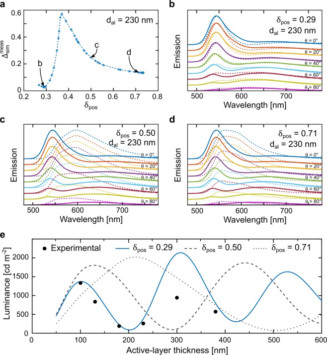
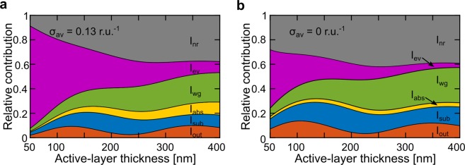
The light-emitting electrochemical cell (LEC) is a contender for emerging applications of light, primarily because it offers low-cost solution fabrication of easily functionalized device architectures. The attractive properties originate in the in-situ formation of electrochemically doped transport regions that enclose an emissive intrinsic region, but the understanding of how this intricate doping structure affects the optical performance of the LEC is largely lacking. We combine angle- and doping-dependent measurements and simulations, and demonstrate that the emission zone in our high-performance LEC is centered at ~30% of the active-layer thickness (dal) from the anode. We further find that the emission intensity and efficiency are undulating with dal, and establish that the first emission maximum at dal ~ 100 nm is largely limited by the lossy coupling of excitons to the doping regions, whereas the most prominent loss channel at the second maximum at dal ~ 300 nm is wave-guided modes.


Conflict of interest statement

The authors declare no competing interests.

Figures

Figure 1
Figure 1
(a) Schematic of the LEC device structure, with the thickness of each layer defined. (b) The angle-resolved optoelectronic measurement setup with the definition of the viewing angle, θ. (c) The measured steady-state voltage as a function of active-layer thickness for the LEC devices driven by a current density of 25 mA cm−2, with the dashed black line representing a linear fit of the experimental data. (d) The width of the intrinsic region, di, (left y-axis) and the fraction of the active layer occupied by the intrinsic region, di/dal, (right y-axis) as a function of the active-layer thickness, as derived with the procedure outlined in the text.
Figure 2
Figure 2
(a) The schematic doping structure of an LEC device operating at steady-state, with the width of the intrinsic region, di, its central position in the active layer, δpos, and the position of the electrodes defined. The steady-state doping-concentration profiles for LEC devices with δpos = 0.29 (solid blue line), δpos = 0.50 (dashed line), and δpos = 0.71 (dotted line). The trivial doping profile for a doping-free device (dash-dotted red line) is included as a reference. The corresponding spatial profiles for (b) the refractive index and (c) the extinction coefficient at λ = 550 nm.
Figure 3
Figure 3
(a) The calculated difference between the measured and simulated data as a function of δpos for the LEC with dal = 230 nm and σav = 0.13 r.u.−1. (bd) The measured (solid lines) and simulated (dashed lines) emission spectra for a set of viewing angles ranging from 0° (top trace) to 80° (bottom trace) for the same device. The position of the emissive intrinsic region in the simulation was δpos = 0.29 (b), δpos = 0.50 (c), and δpos = 0.71 (d). The measured and simulated spectra were normalized with respect to the peak intensity at θ = 0°. (e) The measured (solid circles) and the simulated forward luminance as a function of active-layer thickness for LECs, with the simulated data being distinguished by the selected position of δpos, as defined in the upper inset.
Figure 4
Figure 4
The simulated relative contribution to the total power distribution of (from top to bottom): non-radiative modes (Inr, grey area), evanescently coupled modes (Iev, purple area), wave-guided modes (Iwg, green area), linear absorption (Iabs, yellow area), substrate-bound modes (Isub, blue area), and outcoupled modes (Iout, red area). The simulated data represent (a) the LEC during steady-state operation at σav = 0.13 r.u.−1 and (b) a hypothetical undoped LEC device with σav = 0 r.u.−1.

References

    1. Liang JJ, Li L, Niu XF, Yu ZB, Pei QB. Fully Solution-Based Fabrication of Flexible Light-Emitting Device at Ambient Conditions. Journal of Physical Chemistry C. 2013;117:16632–16639. doi: 10.1021/jp405569q. - DOI
    1. Sandström A, Asadpoordarvish A, Enevold J, Edman L. Spraying Light: Ambient-Air Fabrication of Large-Area Emissive Devices on Complex-Shaped Surfaces. Advanced Materials. 2014;26:4975–4980. doi: 10.1002/adma.201401286. - DOI - PubMed
    1. Sandström A, Dam HF, Krebs FC, Edman L. Ambient fabrication of flexible and large-area organic light-emitting devices using slot-die coating. Nature Communications. 2012;3:1002. doi: 10.1038/ncomms2002. - DOI - PMC - PubMed
    1. Hernandez-Sosa, G. et al. The Compromises of Printing Organic Electronics: A Case Study of Gravure-Printed Light-Emitting Electrochemical Cells. Advanced Materials, 3235–3240, 10.1002/adma.201305541 (2014). - PubMed
    1. Jürgensen N, Zimmermann J, Morfa AJ, Hernandez-Sosa G. Biodegradable Polycaprolactone as Ion Solvating Polymer for Solution-Processed Light-Emitting Electrochemical Cells. Scientific Reports. 2016;6:36643. doi: 10.1038/srep36643. - DOI - PMC - PubMed

Publication types