Review
. 2019 Jul 22;24(14):2651.
doi: 10.3390/molecules24142651.

Metadevices with Potential Practical Applications

Affiliations
Review

Metadevices with Potential Practical Applications

Yafei Li et al. Molecules. .

Abstract

Metamaterials are "new materials" with different superior physical properties, which have generated great interest and become popular in scientific research. Various designs and functional devices using metamaterials have formed a new academic world. The application concept of metamaterial is based on designing diverse physical structures that can break through the limitations of traditional optical materials and composites to achieve extraordinary material functions. Therefore, metadevices have been widely studied by the academic community recently. Using the properties of metamaterials, many functional metadevices have been well investigated and further optimized. In this article, different metamaterial structures with varying functions are reviewed, and their working mechanisms and applications are summarized, which are near-field energy transfer devices, metamaterial mirrors, metamaterial biosensors, and quantum-cascade detectors. The development of metamaterials indicates that new materials will become an important breakthrough point and building blocks for new research domains, and therefore they will trigger more practical and wide applications in the future.

Keywords: detectors; metamaterials; mirrors; nanobiosensors; near-field energy transfer.


Conflict of interest statement

The authors declare no conflict of interest.

Figures

Figure 1
Figure 1
(a) Schematic of experimental setup for near-field energy transfer study. (b) Near-field conductance as a function of gap. Reproduced with permission from [70]. Copyright American Physical Society, 2008.
Figure 2
Figure 2
Near field conductance curves corresponding to five silicon samples with different carrier concentrations. (a) Theoretical calculation and (b) experimental measurement. Reproduced with permission from [73]. Copyright AIP Publishing, 2013.
Figure 3
Figure 3
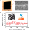
Optical and SEM of nickel nanowires arrays and proof of their loss-free property. (a) Optical and (b) SEM image of the nickel nanowires array. (c) The near field conductance as a function of distance between the nanosphere and nanowires. The top left inset is top view SEM of nanowires array. Reproduced with permission from [84]. Copyright American Chemical Society, 2015.
Figure 4
Figure 4
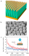
Demonstration of near-field energy transfer. (a) Schematic and (b) SEM image of the exposed nickel nanowires array. (c) The near field thermal conductance as a function of the distance between the nanosphere and AAO template with (red dots) and without (blue dots) exposed nanowires. Reproduced with permission from [84]. Copyright American Chemical Society, 2015.
Figure 5
Figure 5
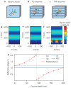
(a) Metamaterial mirrors (MMs) as electric mirror. (b) Flip the electric field of transverse electric (TE)-polarized light on reflection and as magnetic mirror. (c) Flip the magnetic field of transverse magnetic (TM)-polarized light. (df) The electric field distributions of the incident light when it is reflected from (d) a conventional planar silver mirror and (e) grooved silver MMs with TE polarized light and (f) TM polarized light. (g) The effect of groove depth on the reflection phase of different materials. Reproduced with permission from [86]. Copyright Springer Nature, 2014.
Figure 6
Figure 6
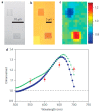
(a) SEM and (b) optical image of silver film with vertical direction (top) and horizontal direction (bottom) groove arrays. (c) Image showing the distribution and size of photocurrent. (d) Plot of photocurrent enhancement factors (blue line). The green line is obtained by replacing each original groove with 10 nm narrow grooves. The red points are real photocurrent enhancement factors, and the error bands are the maximum and minimum photocurrent values in the groove array. Reproduced with permission from [86]. Copyright Springer Nature, 2014.
Figure 7
Figure 7
(a) Electric and (b) magnetic field distributions of flat Au layer and AuNPs array. Reproduced with permission from [87]. Copyright Optical Society of America, 2015.
Figure 8
Figure 8
Properties of silica-Au core-shell mirrors. (a) Calculated impedance and (b) reflection of silica-Au core-shell NP array. (c) The electric field distribution of MMs at SPPs mode 1 and mode 2. Reproduced with permission from [87]. Copyright Optical Society of America, 2015.
Figure 9
Figure 9
The geometry and characteristics of split-ring resonators (SRR) biosensors. (a) Overview SEM and magnified image of U45 SRR array. (b) The transmission spectra of three U-shaped SRRs measured in the experiment (U35 in black, U45 in red, and U55 in blue), compared with (c) Simulate transmission spectra. The electric resonance (ER) and magnetic resonance (MR) modes are marked with black and red asterisks, respectively. (d) Calculated local electric field (|E|4) of three structures. (e) The surface-enhanced Raman scattering (SERS) spectra of single-stranded oligonucleotides attached to three types of U-shaped SRRs. Reproduced with permission from [100]. Copyright American Chemical Society, 2013.
Figure 10
Figure 10
Conformation analysis of the single-stranded oligonucleotides attached to the SRRs in different states. (a) From top to bottom, the transmission spectra of bare U45 SRRs, fixed in thiolated single-stranded DNA in water, then folded into G4 in K+ buffer, and washed by water for 10 min at 90 ℃. Resonance wavelengths are 844, 895, 970 and 889 nm, respectively. The resonant peaks are marked by black arrows. (b) Raman spectra of the above states. The black line is Raman signal of single-stranded oligonucleotides on Au film. Reproduced with permission from [100]. Copyright American Chemical Society, 2013.
Figure 11
Figure 11
SERS spectra of different modified nanoporous gold (NPG) disks. (a) Spectra of MCH functionalized NPG disks immersed in malachite green (MG) solution (black curve), G4-functionalized NPG disks immersed in buffer solution (red curve) and in MG solution (blue curve). (b) Image of different states NPG disks. (c) Corresponding SERS intensity at 1175 cm−1, 1397 cm−1 and 1613 cm−1. Reproduced with permission from [113]. Copyright American Chemical Society, 2016.
Figure 12
Figure 12
SERS spectra with different MG concentrations. (a) Spectra of the MG concentrations from 0.05 nM to 20 μM. (b) SERS intensity at 1175 cm−1, 1397 cm−1 and 1613 cm−1 as a function of MG concentration. Inset is a linear relationship fit between the intensity and the logarithm of MG concentration at 1175 cm−1 at the range of 0.5–2000 nM. Reproduced with permission from [113]. Copyright American Chemical Society, 2016.
Figure 13
Figure 13
The structure of metamaterial detector. The yellow layer on the top is metamaterial region (the green part is SiNx insulation). The coordinate system in the left corner represents the axis direction. Reproduced with permission from [53]. Copyright Springer Nature, 2014.
Figure 14
Figure 14
Comparison of the response spectra between experimental and simulation results. (a) The spectra with a period of 9.15 μm in different polarization directions. (b) Spectrum with period of 11.97 μm of the unpolarized response at low and high frequencies. (cf) The optical responses of the experiment (red) and simulation results (blue dotted) of period 8.54, 9.15, 10.56, and 11.97 μm at the Ex polarization direction. The gray line represents the inter-sub-band transition. Reproduced with permission from [53]. Copyright Springer Nature, 2014.
Figure 15
Figure 15
(a) Photocurrent responsivity of the SRRs coupled device and 45° edge facet coupling device. (b) The photocurrent spectra as a function of wavelength at different polarization angles. Reproduced with permission from [54]. Copyright SpringerOpen, 2016.

Similar articles

Cited by

References

    1. Ishihara K., Suzuki T. Metamaterial Demonstrates Both a High Refractive Index and Extremely Low Reflection in the 0.3-THz Band. J. Infrared Millim. Terahertz Waves. 2017;38:1130–1139. doi: 10.1007/s10762-017-0416-8. - DOI
    1. Yoo S., Park Q.-H. Metamaterials and Chiral Sensing: A Review of Fundamentals and Applications. Nanophotonics. 2019;8:249–261. doi: 10.1515/nanoph-2018-0167. - DOI
    1. Gholipur R., Bahari A. Preparation and Characterization Silver/Zirconium Nickel Oxide Nanocomposites with Negative Electromagnetic Parameters. Opt. Laser Technol. 2017;91:166–174. doi: 10.1016/j.optlastec.2016.12.034. - DOI
    1. Ling F., Zhong Z.Q., Huang R.S., Zhang B. A Broadband Tunable Terahertz Negative Refractive Index Metamaterial. Sci. Rep. 2018;8:9843. doi: 10.1038/s41598-018-28221-3. - DOI - PMC - PubMed
    1. Fegadolli W.S., Pavarelli N., O’Brien P., Njoroge S., Almeida V.R., Scherer A. Thermally Controllable Silicon Photonic Crystal Nanobeam Cavity Without Surface Cladding for Sensing Applications. ACS Photonics. 2015;2:470–474. doi: 10.1021/ph5004863. - DOI

MeSH terms

LinkOut - more resources