Review
. 2019 Jul 12;12(14):2242.
doi: 10.3390/ma12142242.

Native Point Defect Measurement and Manipulation in ZnO Nanostructures

Affiliations
Review

Native Point Defect Measurement and Manipulation in ZnO Nanostructures

Leonard Brillson et al. Materials (Basel). .

Abstract

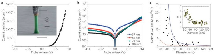
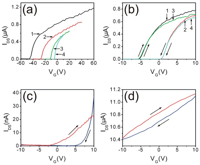
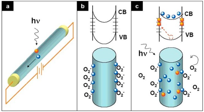
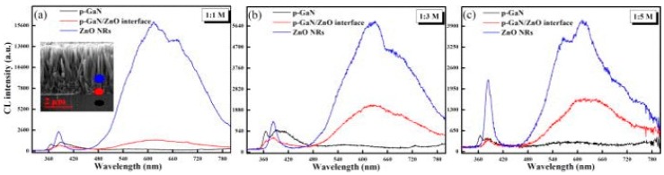
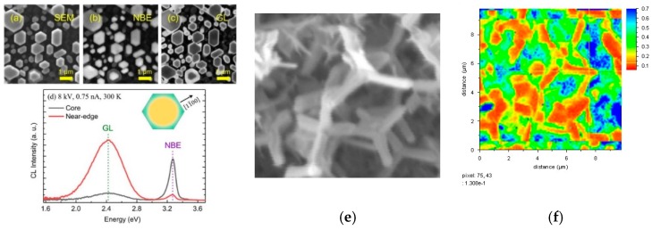
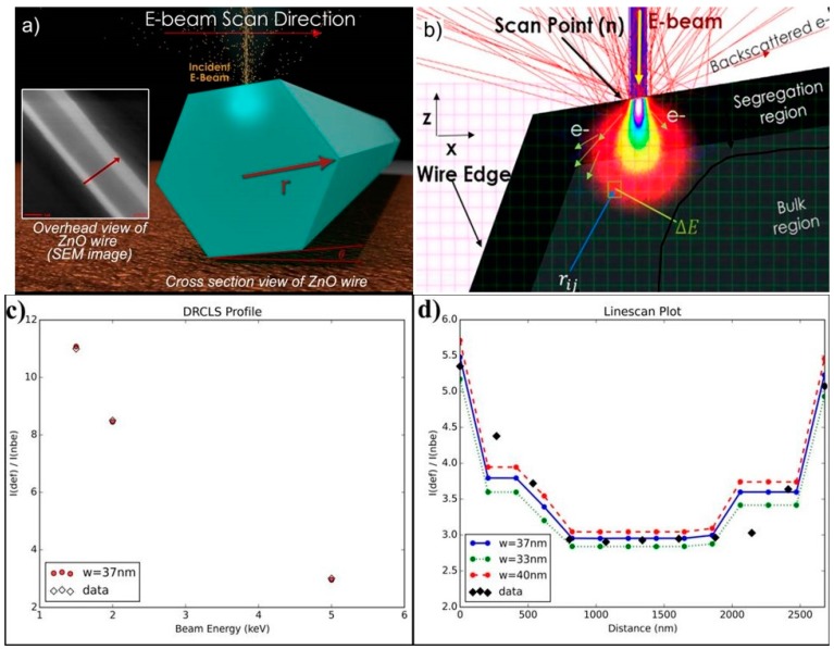
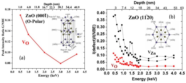
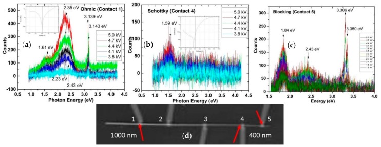
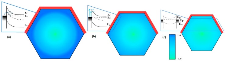
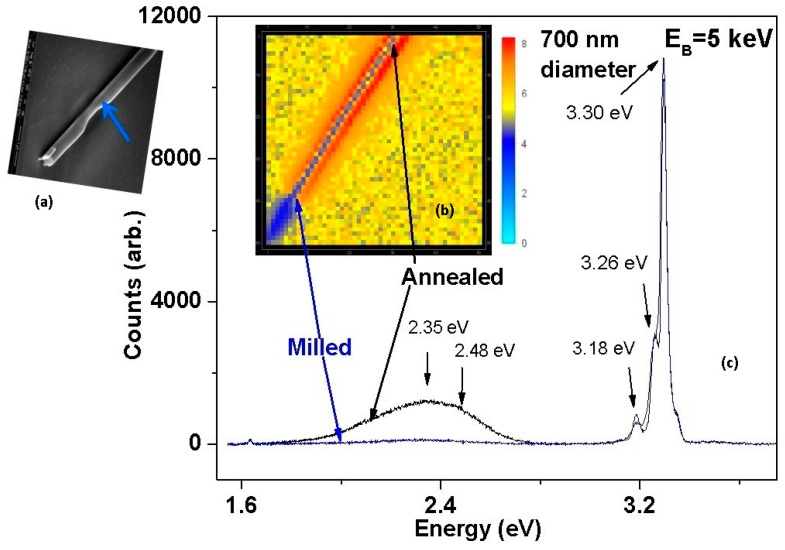
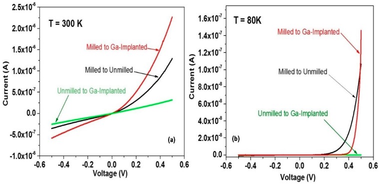
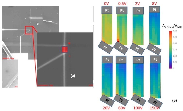
This review presents recent research advances in measuring native point defects in ZnO nanostructures, establishing how these defects affect nanoscale electronic properties, and developing new techniques to manipulate these defects to control nano- and micro- wire electronic properties. From spatially-resolved cathodoluminescence spectroscopy, we now know that electrically-active native point defects are present inside, as well as at the surfaces of, ZnO and other semiconductor nanostructures. These defects within nanowires and at their metal interfaces can dominate electrical contact properties, yet they are sensitive to manipulation by chemical interactions, energy beams, as well as applied electrical fields. Non-uniform defect distributions are common among semiconductors, and their effects are magnified in semiconductor nanostructures so that their electronic effects are significant. The ability to measure native point defects directly on a nanoscale and manipulate their spatial distributions by multiple techniques presents exciting possibilities for future ZnO nanoscale electronics.

Keywords: cathodoluminescence spectroscopy; electronic measurement; interface; nanostructures; nanowires; native point defects.


Conflict of interest statement

The authors declare no conflict of interest.

Figures

Figure 1
Figure 1
(a) End-on Au/Ge nanowire Schottky diode. (b) Current-voltage measurements for contacts to nanowires of different diameter. (c) Calculated conductance dI/dV based on a diameter-dependent (solid line) versus diameter-independent (dashed line) recombination time. Inset shows corresponding ideality factor versus wire diameter. Reprinted with permission from American Physical Society, Ridge, NY, USA [20].
Figure 2
Figure 2
Gate voltage (VG)-dependent, 1 V source-drain bias, source-drain current (Ids(VG) of ZnO nanowire FET under ambient conditions for Ids(VG) sweep ranges (a) ±60 V, ±40 V, ±20 V, and ±10 V for sweeps labelled 1–4, respectively. (b) sweep range ±10 V for a doped and (c) undoped nanowire, and (d) the latter in high vacuum. Reprinted with permission from American Institute of Physics [21].
Figure 3
Figure 3
Influence of surface trap states on oxygen molecule adsorption, charge transfer, and band bending within a nanowire. (a) Photoexcitation increases nanowire free carrier density and conduction, which are reduced (b) by oxygen molecule adsorption, increased band bending, and reduced carrier density inside the wire. (c) Above band gap excitation of the O2—adsorbed wire reduces band bending as additional free carriers recombine with trapped surface charge and O2 molecules desorb. With permission from [26]. Copyright 2007 American Chemical Society.
Figure 4
Figure 4
CL spectra of ZnO nanorod junctions with p-type GaN substrates measured in cross-section. (a) Inset shows a characteristic cross-sectional SEI of the heterostructure with blue, red, and black (from top to bottom) spots indicating spatial locations within the heterostructure corresponding to the blue, red, and black (from top to bottom) spectra in each of the figures. The 625–670 nm (1.85–2 eV) defect intensities relative to the 375 nm (3.3 eV) NBE peak emission increase from (a) 1:1 M to (b) 1:3 M to (c) 1:5 M. With permission from American Institute of Physics [47].
Figure 5
Figure 5
ZnO nanorod (a) SEI, region-of-interest (b) 3.32 eV NBE and (c) 2.46 eV GL intensity maps corresponding to the core and near-edge spectral features in (d). SEI of ZnO tetrapods (e) and corresponding HSI map (f) of NBE-normalized GL intensity extending 50–100 nm into the interior. With permission of John Wiley & Sons (ad) [48] and Springer Nature (e,f) [41].
Figure 6
Figure 6
(a) Illustration of the line-scan CLS measurement process and SEI picture of a typical electron beam track across the ZnO wire diameter. (b) Illustration of electron-hole pair creation geometry and geometric parameters used for the defect profile simulation. (c) Single spot depth dependence measurement of I(defect)/I(NBE) intensity ratio versus incident beam energy EB. (d) 5 keV line-scan data (black dots) and best fit (blue line and dots) showing defect emissions extending nearly 1000 nm into the microwire bulk. Reprinted with permission from the Royal Society of Chemistry [15].
Figure 7
Figure 7
Defect segregation below a ZnO single crystal free surface versus crystal orientation. (a) [0001-] VO (2.5 eV) and (b) [112-0] VZn (1.7–2.1 eV) and VO (2.4–2.5 eV) segregation. Higher VO segregation in O- vs. Zn-polar ZnO also shown in ([52]) Reprinted with permission by American Institute of Physics Refs. ([51,52,53], respectively).
Figure 8
Figure 8
DRCLS of (a) ohmic, (b) Schottky, and (c) blocking contacts on the same ZnO nanowire (d) at locations indicated by arrows. Insets in (a,b) show ohmic and Schottky I–V characteristics, respectively. Deep level emissions at each contact depend strongly on the wire diameter.
Figure 9
Figure 9
Schematic diagrams of band bending at Pt-ZnO nano/microwire contact for (a) 900 nm, (b) 600 nm, and (c) 400 nm diameter wires linked to the interfaces of their corresponding wires. Darker shading signifies higher acceptor density and defect-assisted hopping with increasing radius. With decreasing diameter, interface acceptor density decreases and contact behavior changes from transport by (a) trap-assisted tunneling to (b) Schottky rectification to (c) blocking regions extending radially from multiple faceted surfaces can almost fully deplete the 400 nm diameter nanowire. With permission from [18]. Copyright 2018 American Chemical Society.
Figure 10
Figure 10
(a) SEI, (b) HSI, and (c) DRCL spectra obtained at EB = 5 keV of a 700 nm diameter ZnO nanowire on SiO2 with a wire section milled down to 400 nm to remove segregated defects (lower left) versus a section e-beam annealed to promote additional defects (upper right). With permission from [18]. Copyright 2018 American Chemical Society.
Figure 11
Figure 11
I–V characteristics for pairs of ZnO contacts at (a) 300 K and (b) 80 K. For both temperatures, the milled contact exhibits Schottky rectification versus ohmic conduction of the unmilled contact. With permission from [18]. Copyright 2018 American Chemical Society.
Figure 12
Figure 12
(a) Pt wire layout to apply voltage across two Pt contacts spaced 5 μm apart on a 3 μm diameter ZnO nanowire. (b) HSI maps of normalized defect intensity between Pt electrodes showing segregation of defects toward bottom electrode increasing with increasing applied voltage [60].

References

    1. Look D.C. Recent Advances in ZnO Materials and Devices. Mater. Sci. Eng. B. 2001;80:383–387. doi: 10.1016/S0921-5107(00)00604-8. - DOI
    1. Tsukazaki A., Ohtomo A., Kita T., Ohno Y., Ohno H., Kawasaki M. Quantum Hall Effect in Polar Oxide Heterostructures. Science. 2007;315:1388–1391. doi: 10.1126/science.1137430. - DOI - PubMed
    1. Wang Z.L., Song J.H. Piezoelectric Nanogenerators Based on Zinc Oxide Nanowire Arrays. Science. 2006;312:2420246. doi: 10.1126/science.1124005. - DOI - PubMed
    1. Look D.C., Claflin B. Electrical Optical Properties of ZnO Surfaces. In: Selim F., editor. Zinc Oxide the Future Material for Electronics: A Comprehensive Review on ZnO Physics and Defects. Research Signpost; Kerala, India: 2011. p. 61.
    1. Look D.C. New Developments in ZnO Materials and Devices. Proc. SPIE. 2007;6474:647402–647409.

LinkOut - more resources