. 2019 Jul 23;10(1):3292.
doi: 10.1038/s41467-019-11305-7.

Acoustic radiation pressure for nonreciprocal transmission and switch effects

Affiliations

Acoustic radiation pressure for nonreciprocal transmission and switch effects

Thibaut Devaux et al. Nat Commun. .

Abstract

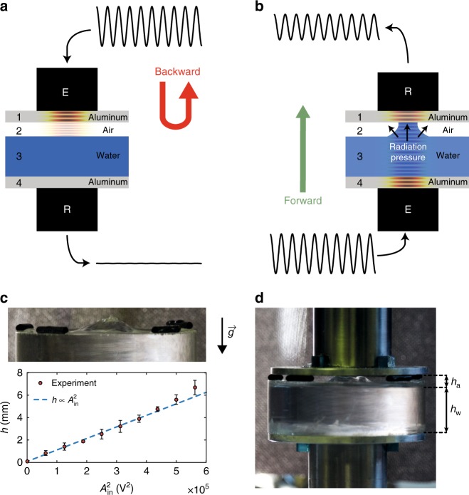
Systems capable of breaking wave transmission reciprocity have recently led to tremendous developments in wave physics. We report herein on a concept that enables one-way transmission of ultrasounds, an acoustic diode, by relying on the radiation pressure effect. This effect makes it possible to reconfigure a multilayer system by significantly deforming a water-air interface. Such a reconfiguration is then used to achieve an efficient acoustic transmission in a specified direction of propagation but not in the opposite, hence resulting in a highly nonreciprocal transmission. The corresponding concept is experimentally demonstrated using an aluminum-water-air-aluminum multilayer system, providing the means to overcome key limitations of current nonreciprocal acoustic devices. We also demonstrate that this diode functionality can even be extended to the design and operations of an acoustic switch, thus paving the way for new wave control possibilities, such as those based on acoustic transistors, phonon computing and amplitude-dependent filters.


Conflict of interest statement

The authors declare no competing interests.

Figures

Fig. 1
Fig. 1
Schematic principle of the concept and a picture of the prototype. a, b Schematic diagrams of the forward (emitter E at the bottom, receiver R at the top) and backward (emitter E at the top, receiver R at the bottom) transmission configurations, respectively. c Radiation pressure effect on the water surface quasi-static deformation. Picture of the water bump, and experimental height as a function of the input electrical amplitude squared (error bars correspond to the standard deviation of 50 data points collected over 10 s for each amplitude); d picture of the tested device when forward transmission is active
Fig. 2
Fig. 2
Temporal signals and amplitude dependence. Transmitted amplitude A+ for an excitation frequency of 2.25 MHz and input amplitude Vin = 450 V, with an air layer thickness ha = 3 mm in: a backward and b forward directions. The inset in a is a close-up of the transmitted signal in the backward direction. c Transmitted amplitude in both the backward (A−) and forward (A+) propagation directions as a function of the emitted amplitude Vin along a cycle of increasing and decreasing amplitudes, for two different excitation frequencies (f1 = 2.05 MHz and f2 = 2.25 MHz) and two different air layer thicknesses: ha = 3 mm in c and ha = 4 mm in d. The diagrams in c, d illustrate the multilayer configuration at the indicated emitted amplitudes. The negative (positive) emitted amplitude horizontal scale corresponds to the peak-to-peak amplitude of the signal emitted in the backward (forward) direction, respectively
Fig. 3
Fig. 3
Experimental frequency response of the diode effect: a Transmitted amplitude in the forward direction (A+) vs. excitation frequency for the diode system with two different air-gap thicknesses, as well as for the reference case without an air gap. The excitation amplitude is Vin = 500 V. b Transmission asymmetry ratio σ = A+2/A2 vs. frequency for two distinct air-gap thicknesses
Fig. 4
Fig. 4
Experimental demonstration of the underlying switch principle: a diagrams of the switch prototype; a phononic crystal (PC) has been added on top of the acoustic diode. The switch working principle is schematically described by the effect of activating a control wave on the transmitted signal wave. b, d emitted electrical waveforms (before a +60 dB amplification by the power amplifier) for a harmonic control signal of frequency kHz and a signal wave in the form of a Gaussian pulse with a carrier frequency f0 = 35 kHz and a spectral full width at half maximum of 5 kHz (b) and 20 kHz (d). c, e output signals transmitted by the switch device. The continuous red lines represent waveforms where the control signal is not turned on, while the continuous blue lines represent signals with the control signal on

References

    1. Jalas D, et al. What is—and what is not—an optical isolator. Nat. Photonics. 2013;7:579–582. doi: 10.1038/nphoton.2013.185. - DOI
    1. Hwang J, et al. Electro-tunable optical diode based on photonic bandgap liquid-crystal heterojunctions. Nat. Mater. 2005;4:383–387. doi: 10.1038/nmat1377. - DOI - PubMed
    1. Wang D-W, et al. Optical diode made from a moving photonic crystal. Phys. Rev. Lett. 2013;110:093901–093905. doi: 10.1103/PhysRevLett.110.093901. - DOI - PubMed
    1. Gallo, K., Assanto, G., Parameswaran, K. R. & Fejer, M. M. All-optical diode in a periodically poled lithium niobate waveguide. Appl. Phys. Lett. 79, 314-3 (2001).
    1. Estep NA, Sounas DL, Soric J, Alu A. Magnetic-free non-reciprocity and isolation based on parametrically modulated coupled-resonator loops. Nat. Phys. 2014;10:923–927. doi: 10.1038/nphys3134. - DOI