Review
. 2019 Aug 6;9(8):1133.
doi: 10.3390/nano9081133.

Nanostructuration of Thin Metal Films by Pulsed Laser Irradiations: A Review

Affiliations
Review

Nanostructuration of Thin Metal Films by Pulsed Laser Irradiations: A Review

Francesco Ruffino et al. Nanomaterials (Basel). .

Abstract

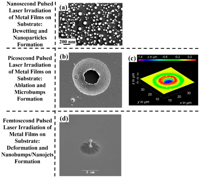
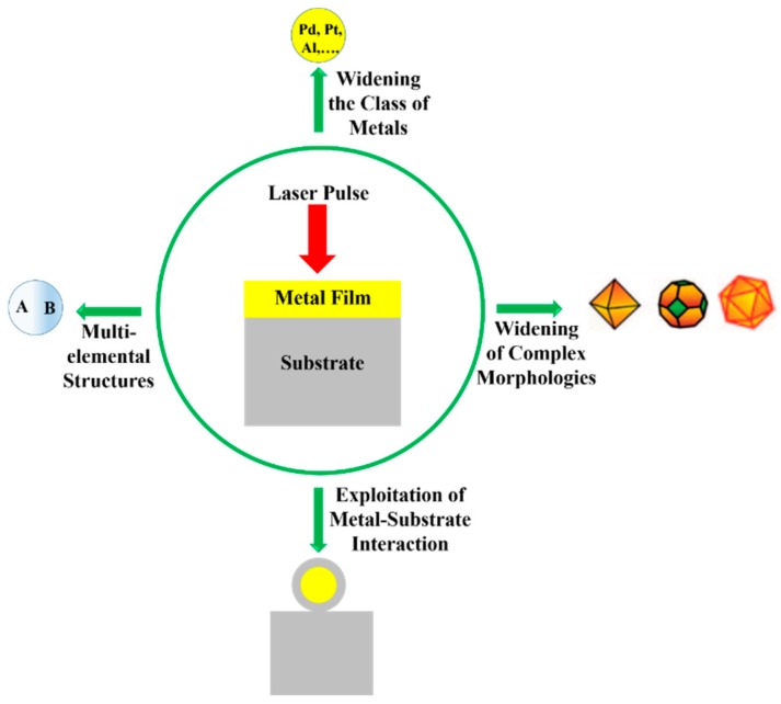
Metal nanostructures are, nowadays, extensively used in applications such as catalysis, electronics, sensing, optoelectronics and others. These applications require the possibility to design and fabricate metal nanostructures directly on functional substrates, with specifically controlled shapes, sizes, structures and reduced costs. A promising route towards the controlled fabrication of surface-supported metal nanostructures is the processing of substrate-deposited thin metal films by fast and ultrafast pulsed lasers. In fact, the processes occurring for laser-irradiated metal films (melting, ablation, deformation) can be exploited and controlled on the nanoscale to produce metal nanostructures with the desired shape, size, and surface order. The present paper aims to overview the results concerning the use of fast and ultrafast laser-based fabrication methodologies to obtain metal nanostructures on surfaces from the processing of deposited metal films. The paper aims to focus on the correlation between the process parameter, physical parameters and the morphological/structural properties of the obtained nanostructures. We begin with a review of the basic concepts on the laser-metal films interaction to clarify the main laser, metal film, and substrate parameters governing the metal film evolution under the laser irradiation. The review then aims to provide a comprehensive schematization of some notable classes of metal nanostructures which can be fabricated and establishes general frameworks connecting the processes parameters to the characteristics of the nanostructures. To simplify the discussion, the laser types under considerations are classified into three classes on the basis of the range of the pulse duration: nanosecond-, picosecond-, femtosecond-pulsed lasers. These lasers induce different structuring mechanisms for an irradiated metal film. By discussing these mechanisms, the basic formation processes of micro- and nano-structures is illustrated and justified. A short discussion on the notable applications for the produced metal nanostructures is carried out so as to outline the strengths of the laser-based fabrication processes. Finally, the review shows the innovative contributions that can be proposed in this research field by illustrating the challenges and perspectives.

Keywords: ablation; deformation; dewetting; femtosecond; metal nanostructures; nanosecond; nanostructuration; picosecond; pulsed laser irradiation; thin metal films.


Conflict of interest statement

The authors declare no conflict of interest.

Figures

Figure 1
Figure 1
The schematic representation of a metal film deposited on a substrate and processed by a laser pulse to induce the film nanostructuration. In the figure, some critical parameters concerning the laser, the film, and the substrate affecting the nanostructuration process are indicated.
Figure 2
Figure 2
The schematic representation, in terms of structuration, of the effect of nano-, pico-, femto-second pulsed laser irradiations on thin metal films deposited on a substrate: (a) a 5 nm-thick Au film deposited on SiO2 and processed by a single pulse of a 12 ns-pulsed laser with a wavelength of 532 nm and a fluence of 750 mJ/cm2 (scanning electron microscopy image). Reproduced with permission from [45]. Copyright Elsevier, 2012; (b,c) a 1 μm-thick Au film deposited on glass and processed by a single pulse of a 10 ps-pulsed laser with a wavelength of 1030 nm and energy of 53 μJ ((a) an optical microscopy in reflection mode and (b) a confocal microscopy). Reproduced with permission from [54]. Copyright Elsevier, 2016; (d) a 60 nm-thick Au film deposited on quartz glass and processed by a single pulse of a 30-fs pulsed laser with a wavelength of 800 nm and energy of 78 nJ (scanning electron microscopy image). Reproduced with permission from [63]. Copyright Springer, 2009.
Figure 3
Figure 3
The heat capacity (per unit volume) Ce, electron-phonon coupling constant G (=Gep), the relaxation time to reach a thermal equilibrium between the electron and phonon systems (τep = τR) for some selected metals (Al, Au, Mo, Ni, Pt) versus the electronic temperature Te. Reproduced with permission from [54]. Copyright Elsevier, 2016
Figure 4
Figure 4
The results of the simulations for the maximum temperature of the electronic system (Tmax,e) and for the maximum temperature of the phonons system (Tmax, ph) as a function of time for Al, Au, Mo, Ni, Pt irradiated by a laser pulse of duration τH = 200 fs (left) or τH = 10 ps (right), laser energy of 1 μJ, laser wavelength of 1028 nm. Reproduced with permission from [54]. Copyright Elsevier, 2016.
Figure 5
Figure 5
The Scanning Electron Microscopy (SEM) images of Ni films with different thicknesses (a) 6.5-nm, (b) 8.2 nm, (c) 11.5 nm, (d) 15 nm) on 320-nm SiO2 and irradiated by a 25 ns-pulsed laser at a wavelength of 248 nm with a fluence of 200 mJ/cm2 (a), 160 mJ/cm2 (b), 140 mJ/cm2 (c), 220 mJ/cm2 (d). Reproduced with permission from [26]. Copyright American Institute of Physics, 2004.
Figure 6
Figure 6
(ad) The size distributions corresponding to the Ni nanoparticles showed in Figure 5. (e) The plot of the mean diameter of the nanoparticles versus the initial film thickness. Reproduced with permission from [26]. Copyright American Institute of Physics, 2004.
Figure 7
Figure 7
The SEM images of 20-nm-thick Mo films (on 235 nm SiO2 thermal grown on Si) treated by laser irradiations (248-nm wavelength, 25-ns pulse duration) at (a) a laser fluence slightly below the critical value for complete dewetting (<660 mJ/cm2) and (b) at a laser fluence slightly above this critical value (>660 mJ/cm2). Reproduced with permission from [34]. Copyright Elsevier, 2007.
Figure 8
Figure 8
The SEM images of (a) 20 nm-thick Au as-deposited on 230 nm SiO2/Si, and, then, the 20 nm-thick Au film laser-processed with (b) a 125 mJ/cm2 fluence, (c) 250 mJ/cm2 fluence, (d) and 430 mJ/cm2 fluence. In addition, SEM images of (e) 15 nm-thick Ag as-deposited on 230 nm SiO2/Si, and, then, the 15 nm-thick Ag film laser-processed with (f) 150 mJ/cm2 fluence, (g) 3000 mJ/cm2 fluence, and (h) 400 mJ/cm2 fluence. Reproduced with permission from [34]. Copyright Elsevier, 2007.
Figure 9
Figure 9
The enthalpy of formation −ΔHf of the oxide per mole of O for some metals. Reproduced with permission from [34]. Copyright Elsevier, 2007.
Figure 10
Figure 10
The plot of the experimentally observed melting fluence for Ag, Au, Mo, and Ni thin films as a function of the film thickness. Reproduced with permission from [27]. Copyright American Physical Society, 2005.
Figure 11
Figure 11
(a) The simulated temperature temporal profile for the surface layer of a 20 nm-thick Ni thin film processed by a 25-ns pulsed laser at 330 mJ/cm2. (b) The plot of the simulated fluence required to melt Ni, Au, and Ag films of different thicknesses. Reproduced with permission from [27]. Copyright American Physical Society, 2005.
Figure 12
Figure 12
(a) The simulated cooling rate coefficient for Ni films of different thicknesses, initially at the melting temperature. (b) The plot of the calculated melting fluence for a 30 nm-thick Ni thin film as a function of the room temperature thermal conductivity of the substrate. The plots refer to a 25 ns pulse and to a laser fluence of 330 mJ/cm2. Reproduced with permission from [27]. Copyright American Physical Society, 2005.
Figure 13
Figure 13
(a) The gaussian intensity profile for the laser used by Ruffino et al. [45] (laser wavelength = 532 nm, pulse duration = 12 ns). (b) Optical photograph of the laser spot on the Au film/SiO2 substrate laser-processed by 1 J/cm2. (cf) Plan-view transmission electron microscopy images taken in the sample irradiated by 1000 mJ/cm2 at increasing distances from the center of the laser spot: (c) >600 μm, (d) between 600 and 300 μm, (e) at about 300 mm, (f) <300 mm. The inset in (f) shows a cross-view transmission electron microscopy image to highlight the shape of the formed nanoparticles. Reproduced with permission from [45]. Copyright Elsevier, 2012.
Figure 14
Figure 14
(a) The enlarged plan-view Transmission Electron Microscopy (TEM) image taken at about 300 mm from the center of the spot to highlight the formation of nanoparticles from wires. (bd) The scheme of the decomposition of an infinite liquid cylinder into an ensemble of particles via a Rayleigh instability. Reproduced with permission from [45]. Copyright Elsevier, 2012.
Figure 15
Figure 15
The evolution of the average Au nanoparticles radius < R > (a) and average surface-to-surface distance < s > (b) versus the laser fluence E. (c) The evolution of the ratio (λ/< R >) = (< s > + 2 < R >/< R >) versus the laser fluence E. Reproduced with permission from [45]. Copyright Elsevier, 2012.
Figure 16
Figure 16
The free energy curve of a metallic film deposited on a non-metallic substrate. Three distinct stability regions can be identified for the film on the basis of the film thickness, named the unstable, metastable, stable thickness regimes. Typically, metal films are unstable in the thickness range 0–1 μm, metastable in the thickness range 1 μm–1 mm, while films with a thickness larger than 1 mm are stable. The inset is a magnified image showing the inflexion point that differentiates the unstable and metastable regions. Reproduced with permission from [37]. Copyright Springer, 2008.
Figure 17
Figure 17
The SEM micrographs presenting the characteristic steps of the morphological evolution of a dewetting 3.5 nm-thick Fe film after pulsed laser irradiation (a wavelength of 266 nm, pulse duration of 9 ns, repletion rate of 50 Hz, a fluence higher than the threshold for melting): (a) 5 pulses, (b) 500 pulses, (c) 10,000 pulses. The fast Fourier transform in the inset of each of the morphological steps depict the short-range spatial order present during each stage of dewetting. Reproduced with permission from [37]. Copyright Springer, 2008.
Figure 18
Figure 18
The plot (Log-Log scales) of the Fe nanoparticle size (r) and spacing (Λ) versus the initial thickness of the deposited Fe film. Dots are experimental data while the lines are the fit of the experimental data by r∝d5/3 and Λ∝d2 (in the figure legend, the film thickness d is indicated by h). Reproduced with permission from [37]. Copyright Springer, 2008.
Figure 19
Figure 19
(a) The plot of the laser energy density threshold for melting Co films on SiO2 versus the film thickness. The plot shows the comparison of experimental measurement (solid circles) with calculations. (b) The calculated temporal profiles’ temperature obtained (using temperature independent parameters) for Co films of different thicknesses on SiO2 under irradiation with 100 mJ/cm2. (c) The calculated temporal profiles’ temperature obtained for Co films of different thicknesses on SiO2 (under 125 mJ/cm2) in the model including the phase change and temperature-dependent parameters. (d) The thermal gradient ∂T/∂h calculated from the thermal model whose magnitude and sign were dependent on the film thickness and time to melt (1, 3, or 9 ns) during the film heating. Reproduced with permission from [33]. Copyright American Physical Society, 2007.
Figure 20
Figure 20
Top row: the SEM images showing the dewetting pattern evolution for a 2 nm-thick Co film irradiated (pulse duration 9 ns) at 200 mJ/cm2 as a function of the number of pulses. The bottom row shows the power spectrum images corresponding to the SEM images in the top row. All the power spectra have an annular structure, indicating a band of spatial frequencies and implying a short-range spatial order. In particular: (a) 10 pulses, (b) 100 pulses, (c) 1000 pulses, and (d) 10 500 pulses. Reproduced with permission from [33]. Copyright American Physical Society, 2007.
Figure 21
Figure 21
The SEM images of (ad) a 2-nm-thick Co film after 100 pulses each of (a) 190 mJ/cm2, (b) 200 mJ/cm2, (c) 220 mJ/cm2, (d) 250 mJ/cm2; (ef) 4.4 nm-thick Co films after irradiation with a fluence of 93 mJ/cm2 but increasing the number of pulses as (e) 10 pulses, (f) 100 pulses, (g) 1000 pulses, (h) 10500 pulses. Reproduced with permission from [33]. Copyright American Physical Society, 2007.
Figure 22
Figure 22
(a) The SEM images of the 7.8 nm-thick Cu ring with a radius of 5 μm and a variable width (125 nm, 200 nm, 259 nm, 352 nm, 407 nm, as indicated in the corresponding images) after 5 pulses (248 nm wavelength, 18 ns pulse duration, 160 mJ/cm2 fluence). Inset: a 60° tilted SEM image of a portion of the corresponding ring. (b) The plot of the mean Cu nanoparticles spacing for fifteen 5 μm-radius and 15 fifteen 10 μm-radius rings as a function of the measured widths. The inset shows the histogram of the droplet spacing (lower right) for 407 nm wide rings of 5 μm radius). Reproduced with permission from [42]. Copyright American Chemical Society, 2011.
Figure 23
Figure 23
(a) The SEM images of the 15 nm-thick Cu ring with a radius of 5 μm and a variable width (108 nm, 145 nm, 203 nm, 303 nm, 380 nm, as indicated in the corresponding images) after 5 pulses (248 nm wavelength, 18 ns pulse duration, 160 mJ/cm2 fluence. (b) The plot of the mean Cu nanoparticles spacing for 15 fifteen 5 μm-radius and 15 fifteen 10-μm radius rings as a function of the measured widths. The inset shows the histogram of the droplet spacing (lower right) for 380 nm wide rings of 5 μm radius.). Reproduced with permission from [42]. Copyright American Chemical Society, 2011.
Figure 24
Figure 24
(a) The SEM images of the 7.8 nm-thick, 1 μm radius copper rings of variable ring widths (270, 580, 900, 1100 nm). (b) Snapshots of nonlinear 2D simulations of these rings in (a) at t = 100 ns (the light blue background shows the original ring. Reproduced with permission from [42]. Copyright American Chemical Society, 2011.
Figure 25
Figure 25
The SEM images of the 15 nm-thick rings ((ac) 303 nm wide and (df) 357 nm wide) laser processed increasing the number of pulses and illustrating the circumferential mass transport competing with the instability of growth and leading to larger than predicted length scales. (gi) 2D simulations of a 350 nm wide ring at different liquid lifetimes which illustrates that the fastest growing modes pinch off and subsequently coarsen the original instability length scale. Reproduced with permission from [42]. Copyright American Chemical Society, 2011.
Figure 26
Figure 26
The array of Ni nanoparticles (on Si substrate) arranged in seven lines and obtained by pulsed laser irradiations (wavelength of 248 nm, pulse duration of 18 ns, fluence of 400 mJ/cm2, five pulses) of seven nanoscale-thick Ni patterned on the substrate by electron beam lithography. Reproduced with permission from [43]. Copyright American Chemical Society, 2011.
Figure 27
Figure 27
The SEM images of a pulsed laser (wavelength of 248 nm, pulse duration of 25 ns, fluence of 420 mJ/cm2) treated thin Ni patterns on the Si substrate. The top images are the initial thin film circle, square and triangle. Subsequent SEM images in each column show the patterns’ evolution after 1, 2, 3, 5, and 10 laser pulses. The bottom image is a tilted view of the pattern after 10 laser pulses. The dashed lines on the top square and triangle illustrate an axis of the lateral contraction from the vertices and the solid lines, indicating the axes from the center of the edges. Reproduced with permission from [105]. Copyright American Institute of Physics, 2008.
Figure 28
Figure 28
The typical ablation structures obtained for Al (first row), Au (second row), Mo (third row), Ni (fourth row), and Pt (fifth row) thin films (deposited on glass), processed by one laser pulse of energy 53 μJ, with a wavelength of 1028 nm, a pulse duration of 200 fs (two columns on left) or 10 ps (two columns on right). For each fixed pulse duration, the first column reports the reflection mode of the optical microscopy images, the second column reports the confocal microscopy images. Reproduced with permission from [54]. Copyright Elsevier, 2016.
Figure 29
Figure 29
The laser-induced periodic surface structures obtained on the Cu (bulk) target after one laser pulse with a wavelength of 355 nm, a pulse duration of 7 ns, a fluence of 0.4 J/cm2. Two irradiation spots with centers separated by about 10 μm can be recognized in the left image. The laser-induced periodic surface structures visible in the right image show an average period of about 300 nm. Reprinted with permission from Reference [109], Elsevier, 2017.
Figure 30
Figure 30
The laser-induced periodic surface structures obtained on Cu (bulk) target after one laser pulse with wavelength = 1064 nm, pulse duration = 7 ns, fluence = 5.5 J/cm2. The irradiation spot can be recognized in the left image. The laser-induced periodic surface structures visible in the right image show an average period of about 580 nm. Reproduced with permission from [109]. Copyright Elsevier, 2017.
Figure 31
Figure 31
The period of the laser-induced periodic surface structures obtained on Cu (bulk): black dots indicate the experimental values (obtained by a single pulse of the 7 ns-pulsed laser with energy = 5.5 J/cm2), the red line indicates the prediction of the model, taking into account the surface plasmon polaritons on a flat metal surface, with the blue squares indicate the predictions of the model, taking into account the realistic surface roughness of the metals surface. Reproduced with permission from [109]. Copyright Elsevier, 2017.
Figure 32
Figure 32
The formation of regular spikes on the Cu film surface (deposited on glass surface) after laser irradiations (42 ps-pulsed lasers with a wavelength of 266 nm and a fluence of 24 mJ/cm2) with (a) 1000, (b) 2000 and (c) 5000 shots. The SEM images are acquired at the center of the laser spot on the sample. Reproduced with permission from [56]. Copyright Elsevier, 2014.
Figure 33
Figure 33
The spatial ordered array of spikes on the Cu film surface (deposited on glass) induced by the laser irradiations (42 ps-pulsed laser with wavelength of 266 nm and fluence of 199 mJ/cm2) with different numbers of laser pulses: (a) 10, (b) 100, (c) 1000, (d) 1000, (e) 5000, (f) 10000. In particular, the images in the first row are acquired at the center of the irradiated region, where the laser fluence is 199 mJ/cm2, while the images in the second row are acquired at the edge of the irradiated region where the laser energy is lower than 199 mJ/cm2. The images in the first row are different due to the increase of the number of the laser pulses (from 10 to 1000). The images in the second row are different due to the increase of the number of pulses which increases from 1000 to 10,000. Reproduced with permission from [56]. Copyright Elsevier, 2014.
Figure 34
Figure 34
The diagrams summarizing the combined effect of number of laser pulses (N) and laser fluence in terms of the characteristic morphological structures obtained on the surface of the Cu film deposited on glass or silicon substrates processed at a wavelength of 266 nm and at a pulse duration of 42 ps. The acronyms are Laser-Induced Periodic Surface Structures (LIPSS), High Spatial Frequency LIPSS (HSFL), Low Spatial Frequency LIPSS (LSFL). Reproduced with permission from [56]. Copyright Elsevier, 2014.
Figure 35
Figure 35
The SEM images of interference patterns produced in Ag film (100 nm-thick) on glass with a single laser pulse (a) and Au film (100 nm-thick) with 3 laser pulses (b) using four interfering beams without a phase difference (wavelength of 1064 nm, energy = 0.7 mJ, period of the holes = 5 μm). Reproduced with permission from [55]. Copyright Elsevier, 2011.
Figure 36
Figure 36
The SEM images showing the results of the single-pulse laser ablation (laser of wavelength 800 nm, pulse duration of 30 fs) of a 100 nm-thick Cr film on glass substrate, increasing the laser energy. The sequences in (a) and (b) are separated by a critical value for the laser energy and above this value Cr droplets ejection is observed. Reproduced with permission from [57]. Copyright Springer, 2003.
Figure 37
Figure 37
The SEM images showing the results of the single-pulse laser ablation (laser of wavelength 800 nm, pulse duration of 30 fs) of a 60 nm-thick Cr film on quartz glass substrate, increasing the laser energy. Reproduced with permission from [58]. Copyright Springer, 2004.
Figure 38
Figure 38
The height of the Au microbumps (solid curve) and nanojet (dashed curve) versus the laser pulse energy (30 fs pulsed laser with 800 nm wavelength). The broken arrows indicate the fact that by starting from 16 nJ of laser energy, the Au modification process evolves to an unstable condition resulting in the destruction of the microbubbles and the nanojets. Reprinted with permission from Reference [58], Springer, 2004 Reproduced with permission from [58]. Copyright Springer, 2004.
Figure 39
Figure 39
The SEM images showing two cases of spatially organized structures fabricated in a 60 nm-thick Au film on quartz by femtosecond laser pulses (30 fs pulsed laser with an 800 nm wavelength). Reproduced with permission from [58]. Copyright Springer, 2004.
Figure 40
Figure 40
The structures obtained by the irradiation of a 60 nm-thick Au film (on glass substrate) with a single laser pulse (wavelength 800 nm, pulse duration 30 fs) having a square-shaped intensity distribution. The laser fluences are 0.190 J/cm2 (a), 0.195 J/cm2 (b), and 0.2 J/cm2 (c). Reproduced with permission from [63]. Copyright Springer, 2009.
Figure 41
Figure 41
The structures obtained by irradiation of a 60 nm-thick Au film (on glass) with a single laser pulse (wavelength 800 nm, pulse duration 30 fs) with an energy of 40 nJ (a), 46 nJ (b), 58 nJ (c), 78 nJ (d). In this case, an achromatic lens was used to focus the gaussian laser beam, having a diameter of 8 mm, on the Au film surface. Reproduced with permission from [63]. Copyright Springer, 2009.
Figure 42
Figure 42
The structures obtained by irradiation of a 60 nm-thick Au film (on glass) with a single laser pulse (wavelength 800 nm, pulse duration 30 fs). In this case, the gaussian laser beam with the diameter of 8 mm has been focused on the sample surface with a 20 mm achromatic lens. The laser pulse energies are indicated in the images and increases from (a) to (j). Reproduced with permission from [66]. Copyright Springer, 2012.
Figure 43
Figure 43
(ae) The tilted SEM images of structures produced on a 60 nm-thick Au film surface by a single 30 fs-pulsed laser pulse. (fo) Time-resolved images of liquid jets formed on a surface of two different liquids after irradiation by a 9 ns-pulsed laser pulse with a 40 μm focus diameter. Images (fj) correspond to a laser pulse energy of 21 μJ and a 4% alginate solution. Images (ko) correspond to a laser pulse energy of 14 μJ and a 3% alginate solution. Reproduced with permission from [66]. Copyright Springer, 2012.
Figure 44
Figure 44
The sequence of pictures illustrating the mechanisms responsible for femtosecond laser-induced formation of structures on a thin Au film on a substrate: the figures from (a) to (e) picture the temporal steps involed in the overall formation process. Reproduced with permission from [66]. Copyright Springer, 2012.
Figure 45
Figure 45
The sequence of SEM images elucidating the formation and evolution of the nanobump array generated on the Au thin film by four interfering femtosecond laser beams. The laser fluence is 87 mJ/cm2 with a wavelength of 780 nm, and a pulse duration of 120 fs (a), 355 fs (b), 741 fs (c), 1220 fs (d). The top left inset illustrates the beam incidence on the film and top right inset illustrates the formation process of the bump. Reproduced with permission from [61]. Copyright Elsevier, 2007.
Figure 46
Figure 46
The evolution (as a function of the laser pulse duration) of the height and diameter of the nanobump as a function of the pulse duration at (a) 87 mJ/cm2 and (b) 114 mJ/cm2 (laser wavelength of 780 nm). Reproduced with permission from [61]. Copyright Elsevier, 2007.
Figure 47
Figure 47
The nanojets array generated at the pulse duration of 2.4 ps and at a fluence of 190 mJ/cm2. Reproduced with permission from [61]. Copyright Elsevier, 2007.
Figure 48
Figure 48
The schematic picture of the computational setup used in molecular dynamics–two temperatures model calculations employed by Ivanov et al. Acronyms: Molecular Dynamics (MD), Two Temperatures Model (TTM), Non-Reflective Boundary (NRB). Reproduced with permission from [62]. Copyright Springer, 2008.
Figure 49
Figure 49
Snapshots from a molecular dynamics-two temperatures model simulation of a 20 nm-thick Ni film deposited onto a transparent substrate and processed by a 200-fs laser pulse focused on a 10 nm spot in the middle of the computational cell. The average fluence absorbed within the beam diameter is 3.1 J/cm2. Atoms are colored according to the local order parameter so that red atoms have local crystalline surroundings, blue atoms belong to the liquid and, in the last snapshot, to small crystallites disoriented with respect to the original crystalline structure of the film. Reproduced with permission from [62]. Copyright Springer, 2008.
Figure 50
Figure 50
The calculated time evolution of the electron and lattice temperatures (a), pressure (b), and velocity in the direction normal to the substrate (c) averaged over a part of the film within 2 nm from the center of the laser spot. The starting changes of pressure and velocity during the first 25 ps of the simulation are shown with a higher resolution in (d). Reproduced with permission from [62]. Copyright Springer, 2008.
Figure 51
Figure 51
The representative SEM images of the surface of Fe films (about 500 nm-thick) on the Si substrate and processed by laser pulses of wavelength 800 nm, pulse duration of 50 fs and increasing the number of pulses from left to right (25, 50, 100, 400) and increasing the laser fluence from bottom to top (0.068, 0.086, 0.108, J/cm2). The number of pulses increases from (a1) to (d1), from (a2) to (d2), from (a3) to (d3), the laser fluence increases from from (a3) to (a1), from (b3) to (b1), from (d3) to (d1). Reproduced with permission from [80]. Copyright Elsevier, 2017.
Figure 52
Figure 52
The schematic representation of a plasmonic solar cell prototype. In the glass/Fluorine-doped Tin Oxide (FTO)/Au nanoparticles (yellow dots) multilayer, the large fraction of radiation transmitted by the transparent layer interacts with the nanoparticles used as sub-wavelength scattering elements to couple and trap the sunlight into an absorbing semiconductor thin film by folding the light into the absorber layer. Reproduced with permission from [50]. Copyright Springer, 2014.
Figure 53
Figure 53
The comparison between the absorbance values of the substrates covered by 5 nm (red curve) or 10 nm of Au (blue curve) and processed by a 12 ns-pulsed laser (1 pulse) with a fluence of 1 J/cm2. The insets show the corresponding SEM images of the Au nanoparticles on the fluorine-doped tin oxide surface and the values of the nanoparticles covered area (FA%). Reproduced with permission from [50]. Copyright Springer, 2014.
Figure 54
Figure 54
The SEM images of the FTO surface covered by the Pd film after the 0.50 J/cm2 laser pulse ((a) 3 nm-thick, (b) 27.9 nm-thick). Reproduced with permission from [52]. Copyright MDPI, 2019.
Figure 55
Figure 55
The Raman spectra corresponding to the bare FTO substrate (black), FTO covered by Pd NPs obtained by the laser irradiation of the 27.9 nm-thick Pd film (red) and of the 17.6 nm-thick Pd film (blue), FTO covered by Pt NPs obtained by the laser irradiation of the 19.5 nm-thick Pt film. The SERS effect can be particularly recognized in the blue spectrum. Reproduced with permission from [52]. Copyright MDPI, 2019.
Figure 56
Figure 56
The colors and topography of the obtained Ag surfaces: (a) The plot of Chroma versus Hue comparing colors obtained using the nonburst (i.e., 1 burst, black circles), burst (i.e., 2 or more bursts with uncontrolled energy distribution, red squares), and flexburst (i.e., 2 or more bursts with controlled energy distributions, blue triangles) coloring methods. (b) Commission Internationale de l’Eclairage (CIE) xy Chromaticity diagram comparing the nonburst (i.e., 1 burst, black circles), burst (i.e., 2 or more bursts with uncontrolled energy distribution, red squares), and flexburst (i.e., 2 or more bursts with controlled energy distributions, blue triangles) coloring methods of (a). (c) SEM images of blue surfaces produced using the nonburst (left), burst (middle), and flexburst (right) coloring methods. The Hue is about the same for all squares (H ≈ 295°) whereas the Chroma values are 22.3, 31.2, and 39.44. Significant nanostructures are observed on the surfaces for the cases of burst and flexburst. The relative energy distribution of the burst pulses is shown as the insets along with the orientation of the electric field (E) applied during laser irradiation. Reproduced with permission from [139]. Copyright Wiley, 2018.
Figure 57
Figure 57
The single-pulse nano-structuration of 500 nm-thick Ag films: (ag) tilted-view SEM images showing the topography of the Ag film increasing the laser energy from 240 to 1200 nJ (i.e., from 1.2 to 8.4 J/cm2 laser fluence); (h) tilted-view false-color SEM image showing the typical single-pulse nanotopography covered by a 500 nm thick Ti protective layer; (ik) tilted SEM images of focused-ion-beam cross-sectional cuts of the three main types of the ablative structures presented in (b,d,f) respectively. The scale bar in all images is 1 μm. Reproduced with permission from [140]. Copyright American Chemical Society, 2016.
Figure 58
Figure 58
The enhancement of spontaneous photoluminescence from R6G molecules on the single nanotextures. (ae) Reference tilted-view and top-view SEM images (two upper-most rows, respectively) of the nano-textured craters and double-scale structures produced at the gradually increasing peak fluence, as well as their surface-enhanced photoluminescence images (two bottom rows) obtained under the lateral oblique excitation (the angle of 75° to the sample normal) of the 10 nm-thick layer of R6G molecules with the s- and p-polarized 532 nm continuous-wave laser source with an average excitation fluence of 6 mW/cm2. The dashed white circles in the surface-enhanced photoluminescence images denote the outer dimensions of the craters and through holes, while the blue and red arrows show the polarization direction of the excitation laser source. (f) Normalized surface-enhanced photoluminescence spectra of the R6G layer measured from the 4-μm wide single crater under the s- and p-polarized lateral irradiation. The gray area shows the photoluminescence spectrum measured from the R6G ethanol solution in the cuvette. (g) Normalized surface-enhanced photoluminescence spectra measured from the R6G layer, covering the single craters presented in (ae) under their p-polarized excitation. Each SEPL spectrum was averaged over 50 of the same spectra measured from similar structures and then normalized on the spectrum measured from the R6G layer, covering a non-irradiated (smooth) Ag-film region of the same size Reproduced with permission from [140]. Copyright American Chemical Society, 2016.
Figure 59
Figure 59
The optical infrared properties of laser-generated arrays of the surface features (nanobumps and microjets) on Au films (50 nm-thick) deposited on silica (laser wavelength of 515 nm, pulse duration of 230 fs). In particular, (a) presents normalized absorbance spectra acquired for the arrays formed by various types of surface textures as well as corresponding side-view SEM image showing the geometry evolution of one of the structures of the array. The square-shape arrays are printed to have an identical number of structures (100 × 100) within and a fixed periodicity of 2 μm. The type of structure is varied by tuning the laser energy (as reported in the SEM images). The scale bar of the SEM images corresponds to 400 nm. (b,c) report the normalized absorbance (1−R) spectra for two fixed types of the surface structures, cone-shape nanobumps and nanojets, in arrays fabricated at various periods. The array period varies from 1.5 to 4 μm and is indicated near each spectrum. The insets demonstrate the cross-section Focused-Ion-Beam cuts showing the real geometry of the structures under study. The scale bar is 200 nm. Noteworthy, the 200-nm thick Ti protective layer was coated above the laser-produced Au textures prior to the FIB milling. In the process of FIB cutting, the redeposition of the Ti material occurs onto the bottom part of the hollow Au structure. Reproduced with permission from [76]. Copyright Elsevier, 2019.
Figure 60
Figure 60
The resonant wavelength λr (a) and resonance modulation amplitude (b) versus the array period measured for several types of the laser-generated structures shown on the SEM images (laser wavelength of 515 nm, pulse duration of 230 fs). The scale bar of the SEM images corresponds to 400 nm. Reproduced with permission from [76]. Copyright Elsevier, 2019.
Figure 61
Figure 61
(A) The reported optical images of directly laser-patterned 3 × 3 mm2 arrays on Ag film (50 nm-thick, on silica) at frequency f = 500 kHz, laser scanning velocity v = 7 m/s, filling factor = 80 lines/mm (corresponding to interline separation of 12 μm), at variable pulse energies of 3 (top), 2.6 (middle) and 2.3 (bottom) μJ, using the standard F-Theta objective with the 100-mm focal length (laser wavelength of 1030 nm, pulse duration of 300 fs). (B,C) The reported of top-view SEM images of separate through microholes in the Ag film at different focusing NA = 0.25 and 0.65, respectively, with the corresponding pulse energies indicated in the bottom corners of the images. Reproduced with permission from [78]. Copyright Elsevier, 2019.
Figure 62
Figure 62
The normalized transmittance spectra of micro-hole gratings (gratings G, fixing the holes diameter to D≈4 μm) on the 50-nm thick Ag (A), Al (B), Cu (C) and Au-Pd alloy (D) films on the CaF2 substrates with variable periods (shown by the same colors as the corresponding spectra), the colored numbers showing the spectral positions of their (1,0), (1,1) and (2,0)-peaks and the red dashed lines showing their evolution versus the hole array period P. Insets: top-view SEM images of the gratings with periods shown in microns in the frames (scale bars can vary). Reproduced with permission from [78]. Copyright Elsevier, 2019.
Figure 63
Figure 63
The picture presenting a summary of the metal nano- and micro-structures which can be produced on surfaces by pulsed-laser processing of thin metal films deposited on substrates and the corresponding potential applications.
Figure 64
Figure 64
The picture presenting some potential outlooks for pulsed-laser irradiations of deposited metal films in view of nano-fabrication: the production of multi-elemental structures by processing multi-elemental films or by exploiting chemical reactivity of the metal film to the substrate, widening the morphology control on the produced structures, and widening the class of processable metals to less-studied metal (such as Pd, Pt, Al).

References

    1. Ashby M.F., Ferreira P.J., Schodek D.L. Nanomaterials, Nanotechnologies and Design. Elsevier; Oxford, UK: 2009.
    1. Binns C. Introduction to Nanoscience and Nanotechnology. Wiley; Hoboken, NJ, USA: 2010.
    1. Tiwari A., Mishra A.K., Kobayashi H., Turner A.P.F. Intelligent Nanomaterials-Processes, Properties, and Applications. Wiley and Scrivener Publishing; Hoboken, NJ, USA: 2012.
    1. Cui Z. Nanofabrication—Principles, Capabilities, and Limits. Springer; New York, NY, USA: 2008.
    1. Tseng A.A. Nanofabrication—Fundamentals and Applications. World Scientific Publishing; Hackensack, NJ, USA: 2008.

LinkOut - more resources