Review
. 2019 Jun 3;6(15):1900522.
doi: 10.1002/advs.201900522. eCollection 2019 Aug 7.

Hybrid Silicon Nanowire Devices and Their Functional Diversity

Affiliations
Review

Hybrid Silicon Nanowire Devices and Their Functional Diversity

Larysa Baraban et al. Adv Sci (Weinh). .

Abstract

In the pool of nanostructured materials, silicon nanostructures are known as conventionally used building blocks of commercially available electronic devices. Their application areas span from miniaturized elements of devices and circuits to ultrasensitive biosensors for diagnostics. In this Review, the current trends in the developments of silicon nanowire-based devices are summarized, and their functionalities, novel architectures, and applications are discussed from the point of view of analog electronics, arisen from the ability of (bio)chemical gating of the carrier channel. Hybrid nanowire-based devices are introduced and described as systems decorated by, e.g., organic complexes (biomolecules, polymers, and organic films), aimed to substantially extend their functionality, compared to traditional systems. Their functional diversity is explored considering their architecture as well as areas of their applications, outlining several groups of devices that benefit from the coatings. The first group is the biosensors that are able to represent label-free assays thanks to the attached biological receptors. The second group is represented by devices for optoelectronics that acquire higher optical sensitivity or efficiency due to the specific photosensitive decoration of the nanowires. Finally, the so-called new bioinspired neuromorphic devices are shown, which are aimed to mimic the functions of the biological cells, e.g., neurons and synapses.

Keywords: biosensors; field‐effect transistors; neuromorphics; photodetectors; silicon nanowires.


Conflict of interest statement

The authors declare no conflict of interest.

Figures

Figure 1
Figure 1
Various functionalities of SiNW devices. The central circle shows the fabrication methods of the SiNW. The second layer shows the different functionalized materials (organic or inorganic) on the SiNW. The outer layer shows their most common applications area.
Figure 2
Figure 2
Organic and SiNW hybrid structures having different organic layers: an organic film coating using molecules, polymers, or ionic films for, e.g., photodetection or neuromorphic applications, a chemically passive coating (to prevent molecule adsorption or to be used as a reference sensor), and bioreceptor coating for specific analyte detection.
Figure 3
Figure 3
SiNW fabrication approaches and examples: bottom‐up (top panel) and top‐down (bottom panel). a) Schematics of bottom‐up growth of nanowires starting from gold nanoparticle seeds. Right panels show an example of a grown nanowire and its catalyst (upper panel, scale bar 20 nm, adapted with permission.85 Copyright 2004, American Chemical Society (ACS) Publications), and two microelectrodes contacted by bottom‐up grown and contact printed parallel nanowires, adapted with permission.30 Copyright 2013, Springer. b) An applied example of an array of individually addressable FETs with bottom‐up grown SiNWs. Adapted with permission.45 Copyright 2005, Nature Publishing Group. c) Parallel contact printing of SiNWs onto target substrate where the device is going to be fabricated. Adapted with permission.30 Copyright 2013, Springer. d) Flexible FET with printed bottom‐up grown SiNWs. Adapted with permission.92 Copyright 2016, Wiley‐VCH. e) Syringe injectable mesh nanoelectronics concept, e‐i) with an array of SiNWs FETs for e‐ii,e‐iii) parallel recording of brain activity at 32 separate sites. e‐i) Adapted with permission.26 Copyright 2018, ACS Publications. e‐ii,e‐iii) Adapted with permission.25 Copyright 2017, ACS Publications. f) Schematics of a typical top‐down fabrication process via EBL. Adapted with permission.99 Copyright 2016, PLoS One. g‐i) EBL fabricated SiNW FET. g‐ii) A comparison of various diameters (24, 16, and 8 nm), showing change from 3D to 1D transport. Adapted with permission.97 Copyright 2017, Nature Publishing Group. h‐i) Linear and h‐ii) honeycomb nanowires, and h‐iii) pH sensitivity comparison showing sensitivity improvement on the second case. Adapted with permission.104 Copyright 2013, IEEE. i) FinFET with i‐i) double‐gate gate‐all‐around, i‐ii) with 20 nm cross section, i‐iii) operating as n‐ or p‐type with the help of polarity control gate electrodes. Adapted with permission.109 Copyright 2012, Institute of Electrical and Electronics Engineers (IEEE).
Figure 4
Figure 4
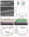
Examples of pH and ion sensing. The left panel shows droplet detection and characterization using SiNW FETs. Adapted with permission.121 Copyright 2016, ACS Publications. a) Nanoliter droplet pH calibration, where the APTES‐modified silicon surface gets protonated at acidic pH and deprotonated at high pH (right inset). The droplet is detected as a current peak with a baseline belonging to the continuous oil phase (left inset). b) Schematics of the droplets containing ongoing enzymatic reactions passing over an FET. c) Recording of the glucose oxidation reaction. The middle panel shows selective ion sensing without the use of selective layers. Adapted with permission.134 Copyright 2018, Nature Publishing Group. d) Schematics of a 0D ISFET (SiNW with the length of 25 nm and width 15 nm), which contains less than 50 charged sites. On its side, a schematic shows the ion interaction model and the potential as a function of the distance for different ion concentrations. e) The low response of such a short nanowire to pH is shown. f) Calibration of various ions in serum. The right panel shows applications of lipid bilayer–coated FETs. g) comparative measurement of an uncoated (blue) and a coated (red) FET with carbon nanotube porins as proton transporters, after incubation for 60 h in simulated milk. Adapted with permission.136 Copyright 2019, ACS Publications. h) Schematics of a nanowire coated with a supported lipid bilayer with an inserted gramicidin channel, through which protons can move unless calcium ions block it. i) pH response of an uncoated FET (red line), a coated FET (blue line), and a coated FET in the presence of calcium ions (black line). Adapted with permission.139 Copyright 2009, National Academy of Sciences of the United States of America.
Figure 5
Figure 5
Applications of cell monitoring with SiNW FETs. a) Recording of glucose consumption of Jurkat leukemia cells using a self‐calibrated FET: a‐i) the self‐calibration mechanism, where an 8‐hydroxypyrene‐1,3,6‐trisulfonyl chloride (HPTS)‐modified nanowire is used. HPTS is excited and deprotonated under illumination at 405 nm, causing a conductance change. The deprotonation degree depends on the pH, and the ratio of the current before and after illumination is considered for the measurement. a‐ii) The concept figure where the cells consume glucose producing acidification; and a‐iii) the results are shown. Adapted with permission.61 Copyright 2013, ACS Publications. b) Antibiotic screening with Escherichia coli bacteria. Adapted with permission.56 Copyright 2017, Royal Society of Chemistry (RSC). b‐i) The concept image, with bacteria producing acidification or alkalization depending on the consumed carbon source. b‐ii) Optical effects of kanamycin (bacteriostatic) and ofloxacin (bactericide) cannot be distinguished. b‐ii,b‐iii) This is achieved with FET measurements, where the continuation of the metabolism after kanamycin injection can be observed, while it is completely stopped with ofloxacin. c) Action potential propagation through a neuron axon aligned along 50 FETs. Adapted with permission.46 Copyright 2006, American Association for the Advancement of Science (AAAS). d) Intracellular action potential recording by silicon nanotube probes grown from SiNW FETs. Adapted with permission.49 Copyright 2011, Nature Publishing Group. d‐i) Conceptual image; d‐ii) germanium nanowire grown from SiNW; d‐iii) final silicon nanotube after SiO2 deposition on the germanium wire; d‐iv) conductance trace over time, reflecting the transition from extracellular to the intracellular recording when the nanotube enters the cell.
Figure 6
Figure 6
a) Importance of specificity and Debye layer. Only charges under the Debye length limit will have influence on FET conductivity. When there are no receptors (left area), pH and the presence of charged molecules (either specific or unspecific) will determine charge carrier movement. In the presence of bioreceptors, only specific targets will bind, avoiding interference on unspecific charges. However, using large receptors, the “caught” charges will remain above the Debye length, showing no conductivity modulation. pH still interacts, though. b) Examples of SiNW surface modification using silanes containing different functional groups where bioreceptors (antibodies or amino‐modified aptamers or single‐stranded DNA molecules) can be immobilized. Inert silanes can also be attached for chemical passivation.
Figure 7
Figure 7
Biosensing with classic bioreceptors (antibody, DNA). a) Rapid cancer cell detection down to 0.1 cells mL−1. Adapted with permission.157 Copyright 2016, ACS Publications, https://pubs.acs.org/doi/full/10.1021/acsnano.5b07136, further permissions related to this figure should be directed to ACS. b) Single Influenza antigen detection with SiNW FETs modified with single antibodies. Adapted with permission.158 Copyright 2014, Wiley‐VCH. The real‐time detection shows three identical peaks independent of the concentration incubated, showing that only one antigen was binding each time. c) DNA detection down to 1 × 10⁻¹⁵ m using SiNWs with triangular cross section. Adapted with permission.159 Copyright 2011, ACS Publications.
Figure 8
Figure 8
Alternative functionalization strategies for improved biodetection. a) Horizontal immobilization of DNA electrostatically deposited on PLL layers. A large detection range between 100 × 10−15 m and 1 × 10⁻⁶ m was obtained. Adapted with permission.111 Copyright 2012, ACS Publications. b) Inner positioning of arginine between glutaraldehyde and APTES to create and electrostatically compressed gap between the receptors and the surface. The detection in real time was possible down to 50 fg mL−1 and the comparison showed clear improvement compared to absence of arginine. Adapted with permission.161 Copyright 2012, ESG.
Figure 9
Figure 9
a) Scanning electron microscopy image and sketch of SiNW modification with antibody fragment decorated gold nanoparticles. The real‐time measurement demonstrates the improved response of the modification, showing stronger signal change. Adapted with permission.53 Copyright 2017, Elsevier. b) Surface co‐immobilization of APTES and PEG, improving the signal as shown in the real‐time measurement graph compared to the surface with only APTES. This strategy allows measuring in high ionic strength, as shown in the right graph with measurements up to 150 × 10−3 m. Adapted with permission.11 Copyright 2015, ACS Publications.
Figure 10
Figure 10
Alternative, smaller bioreceptors. a) DNA detection using PNA, including real‐time measurements down to 10 × 10−15 m (curve 4). Adapted with permission.44 Copyright 2004, ACS Publications. b) Use of aptamers to detect K+ efflux from cells. Graph shows the real‐time measurement where stimulation with α‐amino‐3‐hydroxy‐5‐methyl‐4‐isoxazolepropionic acid (AMPA) is followed by K+ efflux, while 6,7‐dinitroquinoxaline‐2,3‐dione (DNQX) blocking brings the absence of response upon repeated AMPA stimulation. Adapted with permission.57 Copyright 2017, ACS Publications. c) Dopamine detection on pc12 cells under hypoxic stimulation. The right sketch shows the proposed mechanism, by which hypoxia stimulates Ca2+ uptake, which further triggers dopamine release. The real‐time measurements show signal change when hypoxia is generated, and a comparison for different oxygen concentrations, including absence of signal change when Ca2+ channels are blocked with cadmium ions. Adapted with permission.171 Copyright 2013, ACS Publications. d) Measurement improvement using antibody fragments and low receptor density. The increase in the mobility of the receptor due to low density improves the probability of falling inside the Debye limit. When the receptor is small (antibody fragment compared to full antibody), the signal is also improved. Antibodies can be cut by pepsin digestion and cleavage with 2‐MEA, allowing measurements in undiluted PBS, as shown in the graph. Adapted with permission.175 Copyright 2012, ACS Publications.
Figure 11
Figure 11
Alternative measurement modes for FET biosensors. a) Stacked SiNWs for measuring the hysteretic behavior on the memristive properties during biomolecule binding. Adapted with permission.288 Copyright 2017, RSC. b) Conceptual image representing the use of high‐frequency impedance signals, avoiding electrical double layer formation. Adapted with permission.184 Copyright 2015, Nature Publishing Group. c) Application of the impedimetric method to monitor cell growth and differentiation. Adapted with permission.5 Copyright 2015, ACS Publications, https://pubs.acs.org/doi/10.1021/acsami.5b01878, further permissions related to this figure should be directed to ACS. d) Conceptual graph showing hysteresis variation in transfer curve of a SiNW FET according to variations in analyte (thrombin) presence. Adapted with permission.37 Copyright 2018, Multidisciplinary Digital Publishing Institute (MDPI).
Figure 12
Figure 12
CMOS platforms with integrated SiNW FETs. a) Platform comprising poly‐SiNW FETs and temperature sensors with a multiplexer for biosensing of liquid samples. b) The architecture shows the overall schematics of the platform, where the input can be chosen with the multiplexer, amplified, converted to digital signal, and communicated wirelessly for real‐time temperature monitoring and calibration capability for the FETs. Adapted with permission.189 Copyright 2013, RSC. c) CMOS chip with integrated contacts for SiNW FETs, used for biochemical sensing. d‐i) Schematics of the building blocks forming the complete system, including readout electronics, SiNW FET array, and a field‐programmable gate array for data processing and communication to a computer. d‐ii) The picture of the whole packaged system including the polymer fluidic tank for biosensing. d‐iii) Output curves for 27 SiNW FETs. Adapted with permission.188 Copyright 2015, ACS Publications.
Figure 13
Figure 13
Effect of Interfacial trapping of electrons in SiNWs. a) The negative photoconductance of heavily doped SiNW FETs and the trapping phenomena. Adapted with permission.208 Copyright 2017, ACS Publications. b) The photoinduced current change shows trapping could be the major source of the extraction of interfacial trap density using photoconductance analysis of SiNWs. Adapted with permission.213 Copyright 2015, American Institute of Physics (AIP Publishing).
Figure 14
Figure 14
Phototransitive characteristics of SiNWs. a) The planar multi‐SiNW photodetector showing phototransitive gain which is dependent on the photon flux. Adapted with permission.209 Copyright 2008, AIP Publishing. b) Vertically etched SiNW phototransistor and the responsivity under the infra‐red light illumination. Adapted with permission.212 Copyright 2010, ACS Publications.
Figure 15
Figure 15
Organic–inorganic hybrid SiNW photodetectors. a) Optical gate of organic photosensitive molecule (porphyrin)‐coated SiNW FETs. The hybrid shows stronger light‐induced current switching characteristics. The current on/off ratio depends on the thickness of the film. Adapted with permission.3 Copyright 2015, Springer. b) Bioinspired gate using proteins within lipid bilayer of the SiNWFETs. Adapted with permission.10 Copyright 2015, Wiley‐VCH. The light modulates the charge transporting of proteins. c) Molecular embedded SiNW FETs which detect multiple wavelengths. Adapted with permission.236 Copyright 2018, ACS Publications.
Figure 16
Figure 16
Hybrid organic PEDOT:PSS/SiNW heterostructures of solar cells. a) Organic/SiNW hybrid solar cell with inorganic conformal layer. The current–voltage characteristics and EQE of the devices under illumination. Adapted with permission.267 Copyright 2016, ACS Publications. b) Hybrid SiNW solar cell using embedded Ag electrode. Current density–voltage curve and efficiency distribution curves show the increased performance of the solar cell with the embedded electrode. Adapted with permission.268 Copyright 2017, ACS Publications. c) Polymer hybrid solar cell supercapacitor. The supercapacitor is fabricable on the flexible wafer. The inset curves show charging and discharging of the flexible super capacitor with and without solar cell. Adapted with permission.12 Copyright 2017, ACS Publications.
Figure 17
Figure 17
Artificial synapses using Si nanostructures. a) Si nanomembrane (SiNM) transistors gated by chitosan membrane. Ionic excitatory postsynaptic current (EPSC) response to the voltage pulses train applied on the back gate (BG). Adapted with permission.282 Copyright 2018, Wiley‐VCH. b) Recoverable synapse devices using Si finFET. The biological synapse is mimicked using Si FinFET with the electron trajectories during the potentiation and depression. Conductance modulation by the applied pulse cycles. Adapted with permission.13 Copyright 2017, IOP Publishing.

References

    1. Gorton W. S., Proc. IEEE 1998, 86, 658758.
    1. Zheng G., Gao X. P. A., Lieber C. M., Nano Lett. 2010, 10, 3179. - PMC - PubMed
    1. Baek E., Pregl S., Shaygan M., Römhildt L., Weber W. M., Mikolajick T., Ryndyk D. A., Baraban L., Cuniberti G., Nano Res. 2015, 8, 1229.
    1. Dai X., Zhou W., Gao T., Liu J., Lieber C. M., Nat. Nanotechnol. 2016, 11, 776. - PMC - PubMed
    1. Lin S. P., Vinzons L. U., Kang Y. S., Lai T. Y., ACS Appl. Mater. Interfaces 2015, 7, 9866. - PubMed

LinkOut - more resources