. 2019 Jul 25:10:1511-1522.
doi: 10.3762/bjnano.10.149. eCollection 2019.

Rapid thermal annealing for high-quality ITO thin films deposited by radio-frequency magnetron sputtering

Affiliations

Rapid thermal annealing for high-quality ITO thin films deposited by radio-frequency magnetron sputtering

Petronela Prepelita et al. Beilstein J Nanotechnol. .

Abstract

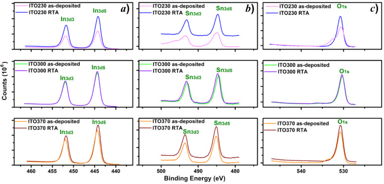
In this work, rapid thermal annealing (RTA) was applied to indium tin oxide (ITO) films in ambient atmosphere, resulting in significant improvements of the quality of the ITO films that are commonly used as conductive transparent electrodes for photovoltaic structures. Starting from a single sintered target (purity 99.95%), ITO thin films of predefined thickness (230 nm, 300 nm and 370 nm) were deposited at room temperature by radio-frequency magnetron sputtering (rfMS). After deposition, the films were subjected to a RTA process at 575 °C (heating rate 20 °C/s), maintained at this temperature for 10 minutes, then cooled down to room temperature at a rate of 20 °C/s. The film structure was modified by changing the deposition thickness or the RTA process. X-ray diffraction investigations revealed a cubic nanocrystalline structure for the as-deposited ITO films. After RTA, polycrystalline compounds with a textured (222) plane were observed. X-ray photon spectroscopy was used to confirm the beneficial effect of the RTA treatment on the ITO chemical composition. Using a Tauc plot, values of the optical band gap ranging from 3.17 to 3.67 eV were estimated. These values depend on the heat treatment and the thickness of the sample. Highly conductive indium tin oxide thin films (ρ = 7.4 × 10⁻⁵ Ω cm) were obtained after RTA treatment in an open atmosphere. Such films could be used to manufacture transparent contact electrodes for solar cells.

Keywords: conductive transparent electrodes; indium tin oxide (ITO) films; optical properties; radio-frequency magnetron sputtering (rfMS); rapid thermal annealing (RTA).


Figures

Figure 1
Figure 1
Cross-sectional SEM images of the cleaved as-deposited (a,c,e) and RTA-processed (b,d,f) ITO films, with measured thickness values of: a) dITO230 = 230 nm, b) dITO230 = 230.4 nm; c) dITO300 = 300.7 nm, d) dITO300 = 300.9 nm, e) dITO370 = 370.5 nm, and f) dITO370 = 371.2 nm.
Figure 2
Figure 2
XRD patterns for the as-deposited and RTA-processed ITO samples.
Figure 3
Figure 3
XPS survey spectra in the range 0–1250 eV acquired from the as-deposited and RTA-treated ITO samples of thickness a) 230 nm, b) 300 nm, and c) 370 nm.
Figure 4
Figure 4
High-resolution a) In 3d, b) Sn 3d and c) O 1s XPS spectra acquired from as-deposited and RTA-treated ITO samples of thickness 230 nm, 300 nm and 370 nm.
Figure 5
Figure 5
Optical transmission spectra for the as-deposited and RTA-treated ITO samples with interference maxima and minima for film thickness of 230 nm, 300 nm, and 370 nm.
Figure 6
Figure 6
a) Refractive index dependence on the wavelength (dispersion) and b) extinction coefficient dependence on the wavelength for the as-deposited and RTA-treated ITO samples.
Figure 7
Figure 7
Dependence of (αhν)2 = f(hν) on the energy of the incident photons, for the as-deposited and RTA-treated ITO samples.
Figure 8
Figure 8
Optical conductivity dependence on the energy of the incident photons for the as-deposited and RTA-treated ITO samples.
Figure 9
Figure 9
Photon energy dependence of the a) real and b) imaginary part of the complex dielectric permittivity for the as-deposited and RTA-treated ITO samples.

References

    1. Lehr D, Wagner M R, Flock J, Reparaz J S, Sotomayor Torres C M, Klaiber A, Dekorsy T, Polarz S. Beilstein J Nanotechnol. 2015;6:2161–2172. doi: 10.3762/bjnano.6.222. - DOI - PMC - PubMed
    1. Kou K-Y, Huang Y-E, Chen C-H, Feng S-W. Beilstein J Nanotechnol. 2016;7:75–80. doi: 10.3762/bjnano.7.9. - DOI - PMC - PubMed
    1. Aydin R. Superlattices Microstruct. 2018;117:46–56. doi: 10.1016/j.spmi.2018.03.022. - DOI
    1. Raj V, dos Santos T S, Rougieux F, Vora K, Lysevych M, Fu L, Mokkapati S, Tan H H, Jagadish C. J Phys D: Appl Phys. 2018;51:395301. doi: 10.1088/1361-6463/aad7e3. - DOI
    1. Krýsová H, Krýsa J, Kavan L. Beilstein J Nanotechnol. 2018;9:1135–1145. doi: 10.3762/bjnano.9.105. - DOI - PMC - PubMed

LinkOut - more resources