. 2019 Aug 15;10(8):536.
doi: 10.3390/mi10080536.

Metal and Polymeric Strain Gauges for Si-Based, Monolithically Fabricated Organs-on-Chips

Affiliations

Metal and Polymeric Strain Gauges for Si-Based, Monolithically Fabricated Organs-on-Chips

William F Quirós-Solano et al. Micromachines (Basel). .

Abstract

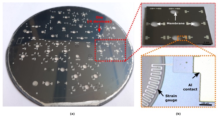
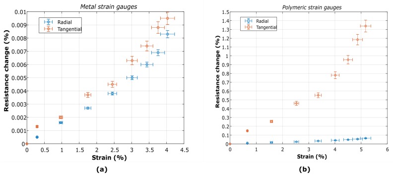
Organ-on-chip (OOC) is becoming the alternative tool to conventional in vitro screening. Heart-on-chip devices including microstructures for mechanical and electrical stimulation have been demonstrated to be advantageous to study structural organization and maturation of heart cells. This paper presents the development of metal and polymeric strain gauges for in situ monitoring of mechanical strain in the Cytostretch platform for heart-on-chip application. Specifically, the optimization of the fabrication process of metal titanium (Ti) strain gauges and the investigation on an alternative material to improve the robustness and performance of the devices are presented. The transduction behavior and functionality of the devices are successfully proven using a custom-made set-up. The devices showed resistance changes for the pressure range (0-3 kPa) used to stretch the membranes on which heart cells can be cultured. Relative resistance changes of approximately 0.008% and 1.2% for titanium and polymeric strain gauges are respectively reported for membrane deformations up to 5%. The results demonstrate that both conventional IC metals and polymeric materials can be implemented for sensing mechanical strain using robust microfabricated organ-on-chip devices.

Keywords: MEMS; PDMS; cell; membranes; organ-on-chip; silicon; strain; stress.


Conflict of interest statement

C.S., N.G. and W.F.Q.-S. are founders of the Startup Company BIOND Solutions B.V. (BI/OND), a spin-off from Delft University of Technology. G.P., R.D. and P.M.S. declare no potential conflict of interests.

Figures

Figure 1
Figure 1
The architecture of the device investigated for stress sensing in a microfabricated PDMS-based OOC platform: Tangential and radial microstructures (strain gauges) on PDMS membranes suspended from a holding silicon frame. The membrane is pneumatically actuated to provide the stretching to a cell culture on its surface.
Figure 2
Figure 2
Strain field of the membranes with radial (a,b) tangential metal strain gauges for a boundary force corresponding to 2 kPa. (c) The curve of the displacement at the center of a membrane with metal (blue line) and polymeric (red line) strain gauges for pressures up to 2 kPa. (d) Corresponding average strain of the membrane.
Figure 3
Figure 3
Main steps of the fabrication process for the integration of Ti strain gauges on PDMS membranes. (a) Deposition of oxide on the wafer front side. (b) Deposition and patterning of the oxide on the wafer back side to define the circular membrane. (c) Deposition and patterning of PI layer for electrical and mechanical isolation. (d) Deposition of Ti and patterning of electrical contacts (Al). (e) Patterning of the metal layer corresponding to the strain gauges (Ti). (f) Deposition of PDMS layer. (g) Deposition and patterning of the Al masking layer and etching of the PDMS layer to open the electrical contacts. (h) Etching of the silicon substrate using a DRIE process. (i) Removal of the landing SiO2. (j) Removal of the masking layer (Al) by wet and dry etching.
Figure 4
Figure 4
The main steps of the process flow developed for the wafer-scale fabrication of polymeric strain gauges. (a) Front and back deposition of the SiO2 oxide and patterning to define the membranes area. (b) Deposition of SiO2 and Ag on the front side patterning to define the electrical contacts. (c) Deposition and patterning of the Al layer to open the electrical contacts to the conductive polymer and to protect the remaining Ag layer for the subsequent etching steps. (d) Deposition and curing of the PEDOT:PSS layer. (e) Deposition and patterning of the Al masking layer. (f) Dry etching of the PEDOT:PSS and removal of Al masking and protective layer from the patterned strain gauges. (g) Deposition of the PDMS layer. (h) Deposition and patterning of the metallic (Al) masking layer and the PDMS layer to open the electrical contacts. (i) Etching of the silicon substrate using a Bosh-based DRIE process. (j) Removal of the landing oxide layer and the masking layer (Al) by wet and dry etching.
Figure 5
Figure 5
Measurement set-up developed to characterize the microfabricated strain gauges. (a) The electrical signal from the strain gauges is acquired by probing them with a standard probe station. The pneumatic actuation is provided simultaneously through a special coupling holder connected to a pressure source. (b) The electrical signal is conditioned and transmitted to a PC for further calculations and data processing.
Figure 6
Figure 6
(a) A completed wafer containing 36 membranes equipped with strain gauges. (b) An optical image of a die containing four devices (top) and a close-up of the released membranes with Ti gauges (bottom). Scale bars: 150 μm (bottom), 3 mm (top).
Figure 7
Figure 7
(a) A completed wafer containing 36 membranes equipped with polymeric strain gauges. (b) Optical images of radial (top) and tangential (bottom) polymeric strain gauges embedded in 10 μm-thick PDMS. (c) A zoom-in perspective illustrating the polymeric strain gauges integrated into the PDMS membranes. Scale bar: 100 μm.
Figure 8
Figure 8
Stationary measurements of resistance change for radial and tangential strain gauges made of (a) titanium (Ti) and (b) PEDOT:PSS. Error bar: 5%.
Figure 9
Figure 9
(a) Displacement in the center of the membranes with metal and polymeric strain gauges measured optically for different pressures set through the pumping system (1–3 kPa). (b) Estimation of the radial strain of the membranes with strain gauges based on the displacement measurements. Error bar: 6%.
Figure 10
Figure 10
Resistance change as function of the strain on the membrane for radial and tangential strain gauges made of (a) titanium (Ti) and (b) PEDOT:PSS.

References

    1. van de Stolpe A. Workshop meeting report Organs-on-Chips: human disease models. Lab Chip. 2013;13:3449. doi: 10.1039/c3lc50248a. - DOI - PubMed
    1. Khoshfetrat Pakazad S. A novel stretchable micro-electrode array (SMEA) design for directional stretching of cells. J. Micromech. Microeng. 2014;24:34003. doi: 10.1088/0960-1317/24/3/034003. - DOI
    1. Gaio N. Cytostretch, an Organ-on-Chip Platform. Micromachines. 2016;7:120. doi: 10.3390/mi7070120. - DOI - PMC - PubMed
    1. Besser R.R. Engineered Microenvironments for Maturation of Stem Cell Derived Cardiac Myocytes. Theranostics. 2018;8:124–140. doi: 10.7150/thno.19441. - DOI - PMC - PubMed
    1. Matsuda T. N-cadherin-mediated cell adhesion determines the plasticity for cell alignment in response to mechanical stretch in cultured cardiomyocytes. Biochem. Biophys. Res. Commun. 2005;326:228–232. doi: 10.1016/j.bbrc.2004.11.019. - DOI - PubMed

LinkOut - more resources