. 2019 Aug 6:13:812.
doi: 10.3389/fnins.2019.00812. eCollection 2019.

Unsupervised Learning on Resistive Memory Array Based Spiking Neural Networks

Affiliations

Unsupervised Learning on Resistive Memory Array Based Spiking Neural Networks

Yilong Guo et al. Front Neurosci. .

Abstract

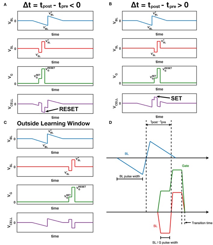
Spiking Neural Networks (SNNs) offer great potential to promote both the performance and efficiency of real-world computing systems, considering the biological plausibility of SNNs. The emerging analog Resistive Random Access Memory (RRAM) devices have drawn increasing interest as potential neuromorphic hardware for implementing practical SNNs. In this article, we propose a novel training approach (called greedy training) for SNNs by diluting spike events on the temporal dimension with necessary controls on input encoding phase switching, endowing SNNs with the ability to cooperate with the inevitable conductance variations of RRAM devices. The SNNs could utilize Spike-Timing-Dependent Plasticity (STDP) as the unsupervised learning rule, and this plasticity has been observed on our one-transistor-one-resistor (1T1R) RRAM devices under voltage pulses with designed waveforms. We have also conducted handwritten digit recognition task simulations on MNIST dataset. The results show that the unsupervised SNNs trained by the proposed method could mitigate the requirement for the number of gradual levels of RRAM devices, and also have immunity to both cycle-to-cycle and device-to-device RRAM conductance variations. Unsupervised SNNs trained by the proposed methods could cooperate with real RRAM devices with non-ideal behaviors better, promising high feasibility of RRAM array based neuromorphic systems for online training.

Keywords: 1T1R RRAM; RRAM (resistive random access memories); STDP; memristor; spiking neural network (SNN); unsupervised learning.


Figures

Figure 1
Figure 1
The architecture of 1T1R crossbar array and 3D fabrication illustration. (A) The 1T1R crossbar array layout. The transistor gates and transistor sources of 1T1R cells in the same row are connected to the G (WL) bus and SL bus respectively. The RRAM top electrodes (TE) of 1T1R cells in the same column are gathered onto the BL bus. (B) The 3D fabrication structure schematic of the 1T1R cell. The bottom electrode (BE) of each RRAM device is connected to the transistor drain node., and the top electrode (TE) is wired with the BL bus. When the transistor gate is open by the high voltage on the WL bus, a positive voltage across BL and SL will help to strengthen conductive filaments in the HfOx/TaOy layer, increasing the RRAM conductance, which is known as the SET operation. FORM operation is similar but with a higher positive voltage across BL and SL, to form the main conductive filaments in the TaOy layer for the first time. RESET requires a reverse operation voltage that tries to cut off the filaments formed in the HfOx layer, thus decreasing the RRAM conductance. (C) Typical switching behavior of our 1T1R device under consecutive identical operation pulses (width = 50 ns) during SET/RESET. VBL = 1.5V, VG = 2.0V, VSL = 0 for SET, and VSL = 1.4V, VG = 4.0V, VBL = 0 for RESET. Abrupt switching is more readily observed during SET.
Figure 2
Figure 2
Schematic for FORWARD/FEEDBACK modes on 1T1R RRAM array. Each Leaky-Integrate-and-Fire neuron (namely post-neuron) is connected to the SL and G nodes and each Poisson neuron (pre-neuron) is connected to the BL. (A) In FORWARD mode, the current stimulated by input pre-spikes can flow through the 1T1R cell and finally arrives at the integrator module of post-neurons (marked as dashed blue curve), where the input information encoded in pre-spikes is conveyed to the post-neurons. (B) When the post-neurons generate output signals, i.e., post-spikes and gate-controls, the circuit changes to the FEEDBACK mode via the control of the two-state switch at SLs. The conductance of RRAM devices could be programmed since the Gate is enabled and there is a voltage across the RRAM devices because of the simultaneous presence of pre-spikes and post-spikes.
Figure 3
Figure 3
Waveform design for BL (pre-spikes), SL (post-spikes) and Gate. The voltage across the 1T1R cell is also displayed as VCELL, which equals to VBL – VSL. (A) A post-spike that fires right before the pre-spike event. (B) A post-spike that fires right after the pre-spike event. (C) A post-spike that fires without overlapping of the pre-spike event. (D) Time parameters of three channels. The transition time of all channels are the same, and SL pulses and Gate pulses have the same synchronized width.
Figure 4
Figure 4
The architecture of SNN and mechanism of LIF neuron. (A) The two-layer SNN architecture. The input layer is responsible for converting input images into spike trains. Poisson neurons are used in this layer. The spikes generated by the input layer are transmitted to the synapses in the middle, fully connecting the input neurons and the output neurons. The synapses modulate the received spikes (defined as pre-spikes) by their weights and pass the spikes to the output layer. LIF neurons in the output layer process the spikes and generate output spikes properly. The mechanism of LIF neuron is explained in (B). The output spikes (defined as post-spikes) are passed back to the corresponding synapses and tune the synapse weights via STDP rule. Additionally, output spikes are broadcasted among output neurons through the lateral inhibition paths, allowing competition during learning. (B) LIF neuron firing mechanism. The LIF neuron has an internal state, i.e., membrane potential. It integrates on the presence of received input spikes and decays exponentially with a time constant τmem. Once the membrane potential reaches a certain threshold Vth, it fires a spike at the output port and the membrane potential is reset to the resting potential Vrest. The fired LIF neuron itself then enters into a short refractory period, when its membrane potential holds at Vrest and does not respond to any recent input spikes.
Figure 5
Figure 5
The STDP model curves of different W states. The potentiation of lower conductance states is stronger than that of higher conductance states, and vice versa for the depression process. Model parameters: A+ = 1.0, A = 0.6, τ+ = τ = 150 ns, Wmax = 50 μS, Wmin = 10 μS. A is set to be smaller than A+, which fits the experimental behavior of RRAM devices in Figure 6.
Figure 6
Figure 6
Experimentally measured STDP characteristic of our 1T1R devices, compared with the model. The waveform parameters of BL, SL, G pulses applied on the devices: VBL+ = 0.6 V, VBL = –1.0 V, VSL+ = 1.3 V, VSL = –1.0 V, VGRESET = 4.0 V, VGSET = 1.0 V, pulse width of VBL = 500 ns, pulse width of VSL and VG = 50 ns, all transition time = 20 ns. The model parameters used here to compare with experimental data are the same as those listed in Figure 5: A+ = 1.0, A = 0.6, τ+ = τ = 150ns, Wmax = 50 μS, Wmin = 10 μS. (A) The experimentally measured data on 1T1R devices (blue points with errorbar) via Keithley 4200A-SCS equipment, and model-predicted STDP curve, around W state of 15.3 μS. Each plotted experimental data point is the average relative conductance change of over 100 trials, and the standard deviation is shown by the corresponding errorbar. In each trial, the device under test is fine-tuned to the target conductance state first, and then pulses are applied to device terminals for once, finally the conductance change is measured. (B) Measured STDP and modeled STDP around W state of 25.1 μS. (C) Measured STDP and modeled STDP around W state of 35.3 μS. (D) Measured STDP and modeled STDP around W state of 45.1 μS.
Figure 7
Figure 7
Block diagram of pattern/background phases and greedy training methods for learning one single image. The left and the right column represent the pattern phase and background phase respectively. The dashed lines annotated with number show the different timing when spikes arrive at the synapses. The pre-spikes in the pattern phase (1) arrive first, then the post-spikes from LIF neurons (2), and finally the pre-spikes generated by the Poisson neurons in the background phase (3). This spikes arriving sequence allows potentiation during pattern phases [synapses modulated by (1) and (2)], and depression during background phases [synapses modulated by (2) and (3)].
Figure 8
Figure 8
Greedy training and pattern/background phases. (A) The schematic of greedy training. Each row with the time axis represents the spiking activity of one neuron over time. Spikes are marked out by the blue vertical arrows. There are two phases for each image stimuli. During the pattern phase, the input neuron corresponding to the pattern pixels are more likely to fire spikes. The pattern phase continues until any of the LIF neurons at the output layer spikes. The LIF neuron's spike switches the input layer into the background phase immediately, allowing the background pixels to strongly stimulate the Poisson neurons. Therefore, the learning window shown by the gray shaded area could help the synapses learn the pattern and forget the irrelevant background efficiently. (B) The firing probability map of Poisson neurons in one single time step. This subfigure shows that the neurons corresponding to the “0” pattern have a higher firing probability during the pattern phase. (C) The firing probability of all pixels during the background phase. The Poisson neurons associated with background pixels are strongly stimulated during the background phase, to enable efficient forgetting of the network.
Figure 9
Figure 9
Comparison between the proposed training method (GREEDY) and conventional training method (CONVENTIONAL) on learning one single pattern. (A) Error rate of pattern pixels versus training epochs of greedy training. (B) Error rate of pattern pixels versus training epochs of conventional training. The convergence of conventional training with large learning rates is much worse than that of greedy training. (C) Error rate of background pixels versus training epochs of greedy training. (D) Error rate of background pixels versus training epochs of conventional training.
Figure 10
Figure 10
Training result on MNIST recognition. (A) The normalized weight map corresponding to 50 post-neurons. Most patterns of 10 digits are impressively learned without any supervision. (B) Testing accuracy on MNIST testing set of 10,000 unseen images during training. The overall testing accuracy is around 76.8%, and most of the categories could be classified with acceptable accuracy.
Figure 11
Figure 11
(A) Heat map of the update counts for each synapse after learning 60,000 MNIST training images. The maximum is <200, which could be ignored for endurance related problems. (B) Impact of array failure rate. A simple SNN of 4 output neurons to recognize 1,000 “0,” “1” images is simulated. The failed devices are kept at the initial state and do not respond to any input. The failure rate could have an impact on the convergence, and 30% failure rate can be tolerated in this application. (C) Using algorithm-level parameters to compensate for the common asymmetric switching behaviors for RRAM devices. For the solid red curve, double the background firing rate factor leads to similar performance with balanced switching conditions.

References

    1. Agarwal S., Plimpton S. J., Hughart D. R., Hsia A. H., Richter I., Cox J. A., et al. (2016). Resistive memory device requirements for a neural algorithm accelerator, in 2016 International Joint Conference on Neural Networks (IJCNN) (Vancouver, BC: IEEE; ), 929–938. 10.1109/IJCNN.2016.7727298 - DOI
    1. Ambrogio S., Balatti S., Milo V., Carboni R., Wang Z., Calderoni A., et al. (2016). Novel rram-enabled 1t1r synapse capable of low-power stdp via burst-mode communication and real-time unsupervised machine learning, in 2016 IEEE Symposium on VLSI Technology (Honolulu, HI: IEEE; ), 1–2. 10.1109/VLSIT.2016.7573432 - DOI
    1. Ambrogio S., Balatti S., Nardi F., Facchinetti S., Ielmini D. (2013). Spike-timing dependent plasticity in a transistor-selected resistive switching memory. Nanotechnology 24:384012. 10.1088/0957-4484/24/38/384012 - DOI - PubMed
    1. Bi G.-q., Poo M.-m. (1998). Synaptic modifications in cultured hippocampal neurons: dependence on spike timing, synaptic strength, and postsynaptic cell type. J. Neurosci. 18, 10464–10472. - PMC - PubMed
    1. Boybat I., Le Gallo M., Nandakumar S. R., Moraitis T., Parnell T., Tuma T., et al. . (2018). Neuromorphic computing with multi-memristive synapses. Nat. Commun. 9:2514. 10.1038/s41467-018-04933-y - DOI - PMC - PubMed

LinkOut - more resources