. 2017 Jun 28;2(6):2985-2993.
doi: 10.1021/acsomega.7b00041. eCollection 2017 Jun 30.

Piezoresistive Response of Quasi-One-Dimensional ZnO Nanowires Using an in Situ Electromechanical Device

Affiliations

Piezoresistive Response of Quasi-One-Dimensional ZnO Nanowires Using an in Situ Electromechanical Device

Sören Kaps et al. ACS Omega. .

Abstract

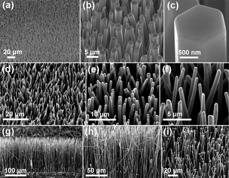
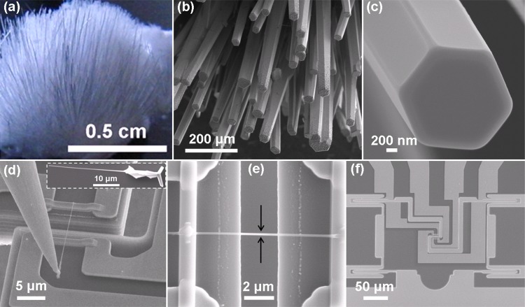
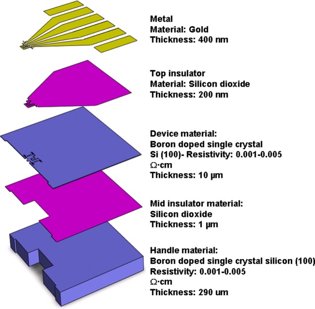
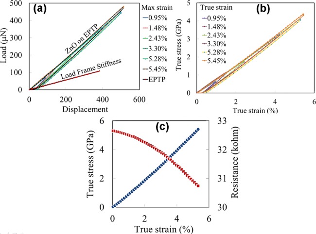
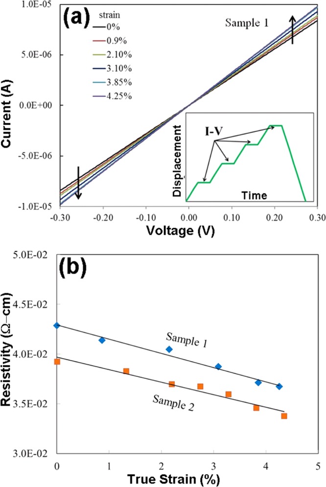
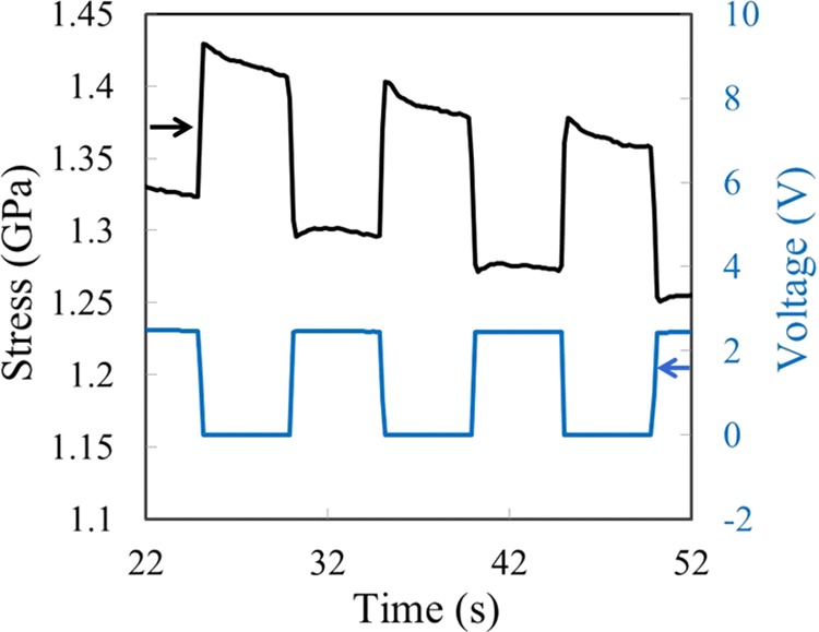
Quasi-one-dimensional structures from metal oxides have shown remarkable potentials with regard to their applicability in advanced technologies ranging from ultraresponsive nanoelectronic devices to advanced healthcare tools. Particularly due to the piezoresistive effects, zinc oxide (ZnO)-based nanowires showed outstanding performance in a large number of applications, including energy harvesting, flexible electronics, smart sensors, etc. In the present work, we demonstrate the versatile crystal engineering of ZnO nano- and microwires (up to centimeter length scales) by a simple flame transport process. To investigate the piezoresistive properties, particular ZnO nanowires were integrated on an electrical push-to-pull device, which enables the application of tensile strain and measurement of in situ electrical properties. The results from ZnO nanowires revealed a periodic variation in stress with respect to the applied periodic potential, which has been discussed in terms of defect relaxations.


Conflict of interest statement

The authors declare no competing financial interest.

Figures

Figure 1
Figure 1
SEM morphologies at increasing magnifications (left to right, low to high) of different Q1D ZnO nano- and microwires synthesized by the FTS approach on Si substrates. (a–c) Homogeneous array of hexagonally faceted Q1D ZnO nanowires. (d–f) Array of Q1D ZnO nano- and microwires with smooth surfaces. (g–i) Side-view SEM images of a dense array of relatively longer (>200 μm length) Q1D ZnO nano- and microwires grown on a Si substrate. These Q1D ZnO microwires are very well interconnected with the base and are almost homogeneous in diameter (bottom to top) with a sharp needle-like tip at their ends. The growth of smaller flower-like ZnO nanostructures on their tips is mainly due to secondary growth (the denser array of wires favors growth on the tips).
Figure 2
Figure 2
Q1D ZnO nano- and microwires from one particular synthesis batch were selected for electrical push-to-pull (E-PTP) studies. (a) Digital photograph of a typical edge of a Si wafer where a bunch of Q1D ZnO wires are grown after the FTS process. (b, c) Typical SEM images from the synthesized Q1D ZnO nano- and microwires at low and high magnifications, respectively. ZnO nanowires were carefully harvested from the bunch (a) and mounted on the E-PTP device. Representative SEM images (d–f) of the mounted (using a nanomanipulator) Q1D ZnO nanowire on the E-PTP device.
Figure 3
Figure 3
Schematic of an E-PTP device shows the dimensions and materials in different layers.
Figure 4
Figure 4
(a, b) Load–displacement and stress–strain curves of Q1D ZnO nanowire tensile experiments at different strains. (c) Stress–strain and resistance–strain curves obtained during tensile experiments of a Q1D ZnO nanowire. A constant voltage of 0.5 V was applied during the test and the current was measured.
Figure 5
Figure 5
(a) IV characteristic curves obtained from a 1D ZnO nanowire 1 showing the change in slope with applied strain. (b) Resistivity vs strain curve showing a decrease in the electrical resistivity of 14.2% in sample 1 and 13.9% in sample 2.
Figure 6
Figure 6
Variation in stress in the Q1D nanowire under periodic potentials.

References

    1. Friedman R. S.; McAlpine M. C.; Ricketts D. S.; Ham D.; Lieber C. M. Nanotechnology: High-speed Integrated Nanowire Circuits. Nature 2005, 434, 1085.10.1038/4341085a. - DOI - PubMed
    1. Goldberger J.; Sirbuly D. J.; Law M.; Yang P. ZnO Nanowire Transistors. J. Phys. Chem. B 2005, 109, 9–14. 10.1021/jp0452599. - DOI - PubMed
    1. Thelander C.; Agarwal P.; Brongersma S.; Eymery J.; Feiner L. F.; Forchel A.; Scheffler M.; Riess W.; Ohlsson B. J.; Gösele U.; et al. Nanowire-based One-dimensional Electronics. Mater. Today 2006, 9, 28–35. 10.1016/S1369-7021(06)71651-0. - DOI
    1. Patolsky F.; Timko B. P.; Zheng G.; Lieber C. M. Nanowire-based Nanoelectronic Devices in the Life Sciences. MRS Bull. 2007, 32, 142–149. 10.1557/mrs2007.47. - DOI
    1. Yan R.; Gargas D.; Yang P. Nanowire Photonics. Nat. Photonics 2009, 3, 569–576. 10.1038/nphoton.2009.184. - DOI