In Situ SiO2 Passivation of Epitaxial (100) and (110)InGaAs by Exploiting TaSiO x Atomic Layer Deposition Process
- PMID: 31458140
- PMCID: PMC6643752
- DOI: 10.1021/acsomega.8b02314
In Situ SiO2 Passivation of Epitaxial (100) and (110)InGaAs by Exploiting TaSiO x Atomic Layer Deposition Process
Abstract
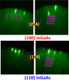
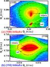
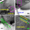
In this work, an in situ SiO2 passivation technique using atomic layer deposition (ALD) during the growth of gate dielectric TaSiO x on solid-source molecular beam epitaxy grown (100)In x Ga1-x As and (110)In x Ga1-x As on InP substrates is reported. X-ray reciprocal space mapping demonstrated quasi-lattice matched In x Ga1-x As epitaxy on crystallographically oriented InP substrates. Cross-sectional transmission electron microscopy revealed sharp heterointerfaces between ALD TaSiO x and (100) and (110)In x Ga1-x As epilayers, wherein the presence of a consistent growth of an ∼0.8 nm intentionally formed SiO2 interfacial passivating layer (IPL) is also observed on each of (100) and (110)In x Ga1-x As. X-ray photoelectron spectroscopy (XPS) revealed the incorporation of SiO2 in the composite TaSiO x , and valence band offset (ΔE V) values for TaSiO x relative to (100) and (110)In x Ga1-x As orientations of 2.52 ± 0.05 and 2.65 ± 0.05 eV, respectively, were extracted. The conduction band offset (ΔE C) was calculated to be 1.3 ± 0.1 eV for (100)In x Ga1-x As and 1.43 ± 0.1 eV for (110)In x Ga1-x As, using TaSiO x band gap values of 4.60 and 4.82 eV, respectively, determined from the fitted O 1s XPS loss spectra, and the literature-reported composition-dependent In x Ga1-x As band gap. The in situ passivation of In x Ga1-x As using SiO2 IPL during ALD of TaSiO x and the relatively large ΔE V and ΔE C values reported in this work are expected to aid in the future development of thermodynamically stable high-κ gate dielectrics on In x Ga1-x As with reduced gate leakage, particularly under low-power device operation.
Conflict of interest statement
The authors declare no competing financial interest.
Figures


References
-
- Chau R.; Datta S.; Doczy M.; Doyle B.; Jin B.; Kavalieros J.; Majumdar A.; Metz M.; Radosavljevic M. Benchmarking Nanotechnology for High-performance and Low-power Logic Transistor Applications. IEEE Trans. Nanotechnol. 2005, 4, 153–158. 10.1109/tnano.2004.842073. - DOI
-
- Takagi S.; Iisawa T.; Tezuka T.; Numata T.; Nakaharai S.; Hirashita N.; Moriyama Y.; Usuda K.; Toyoda E.; Dissanayake S. Carrier-Transport-Enhanced Channel CMOS for Improved Power Consumption and Performance. IEEE Trans. Electron Devices 2008, 55, 21–39. 10.1109/ted.2007.911034. - DOI
-
- Radosavljevic M.; Chu-Kung B.; Corcoran S.; Hudait M. K.; Dewey G.; Fastenau J. M.; Kavalieros J.; Liu W. K.; Lubyshev D.; Metz M.; Millard K.; Rachmady W.; Shah U.; Chau R.. Advanced High-K Gate Dielectric for High-Performance Short-Channel In0.7Ga0.3As Quantum Well Field Effect Transistors on Silicon Substrate for Low Power Logic Applications. IEDM Technical Digest, 2009; pp 319–322.
-
- Radosavljevic M.; Dewey G.; Fastenau J. M.; Kavalieros J.; Kotlyar R.; Chu-Kung B.; Liu W. K.; Lubyshev D.; Metz M.; Millard K.; Mukherjee N.; Pan L.; Pillarisetty R.; Rachmady W.; Shah U.; Chau R.. Non-planar, Multi-gate InGaAs Quantum Well Field Effect Transistors With High-k Gate Dielectric and Ultra-scaled Gate-to-drain/Gate-to-source Separation for Low Power Logic Applications. IEDM Technical Digest, 2010; pp 126–129.
-
- Radosavljevic M.; Dewey G.; Basu D.; Boardman J.; Chu-Kung B.; Fastenau J. M.; Kabehie S.; Kavalieros J.; Le V.; Liu W. K.; Lubyshev D.; Metz M.; Millard K.; Mukherjee N.; Pan L.; Pillarisetty R.; Rachmady W.; Shah U.; Then H. W.; Chau R.. Electrostatics Improvement in 3-D Tri-gate Over Ultra-Thin Body Planar InGaAs Quantum Well Field Effect Transistors with High-K Gate Dielectric and Scaled Gate-to-Drain/Gate-to-Source Separation. IEDM Technical Digest, 2011; pp 765–768.
LinkOut - more resources
Full Text Sources
Research Materials
Miscellaneous

