Atomic Layer Deposition of Nickel Using a Heteroleptic Ni Precursor with NH3 and Selective Deposition on Defects of Graphene
- PMID: 31460211
- PMCID: PMC6648170
- DOI: 10.1021/acsomega.9b01003
Atomic Layer Deposition of Nickel Using a Heteroleptic Ni Precursor with NH3 and Selective Deposition on Defects of Graphene
Abstract
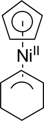
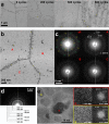
Atomic layer deposition (ALD) of Ni was demonstrated by introducing a novel oxygen-free heteroleptic Ni precursor, (η3-cyclohexenyl)(η5-cyclopentadienyl)nickel(II) [Ni(Chex)(Cp)]. For this process, non-oxygen-containing reactants (NH3 and H2 molecules) were used within a deposition temperature range of 320-340 °C. Typical ALD growth behavior was confirmed at 340 °C with a self-limiting growth rate of 1.1 Å/cycle. Furthermore, a postannealing process was carried out in a H2 ambient environment to improve the quality of the as-deposited Ni film. As a result, a high-quality Ni film with a substantially low resistivity (44.9 μΩcm) was obtained, owing to the high purity and excellent crystallinity. Finally, this Ni ALD process was also performed on a graphene surface. Selective deposition of Ni on defects of graphene was confirmed by transmission electron microscopy and atomic force microscopy analyses with a low growth rate (∼0.27 Å/cycle). This unique method can be further used to fabricate two-dimensional functional materials for several potential applications.
Conflict of interest statement
The authors declare no competing financial interest.
Figures


References
-
- Vij V.; Sultan S.; Harzandi A. M.; Meena A.; Tiwari J. N.; Lee W.-G.; Yoon T.; Kim K. S. Nickel-Based Electrocatalysts for Energy-Related Applications: Oxygen Reduction, Oxygen Evolution, and Hydrogen Evolution Reactions. ACS Catal. 2017, 7, 7196–7225. 10.1021/acscatal.7b01800. - DOI
-
- Iwai H.; Ohguro T.; Ohmi S.-I. Nisi Salicide Technology for Scaled Cmos. Microelectron. Eng. 2002, 60, 157–169. 10.1016/S0167-9317(01)00684-0. - DOI
-
- Kittl J. A.; Lauwers A.; Chamirian O.; Van Dal M.; Akheyar A.; De Potter M.; Lindsay R.; Maex K. Ni- and Co-Based Silicides for Advanced Cmos Applications. Microelectron. Eng. 2003, 70, 158–165. 10.1016/S0167-9317(03)00370-8. - DOI
-
- Johnson R. W.; Hultqvist A.; Bent S. F. A Brief Review of Atomic Layer Deposition: From Fundamentals to Applications. Mater. Today 2014, 17, 236–246. 10.1016/j.mattod.2014.04.026. - DOI
LinkOut - more resources
Full Text Sources
Research Materials
Miscellaneous

