

Long valley lifetime of dark excitons in single-layer WSe2
- PMID: 31492874
- PMCID: PMC6731252
- DOI: 10.1038/s41467-019-12129-1
Long valley lifetime of dark excitons in single-layer WSe2
Abstract
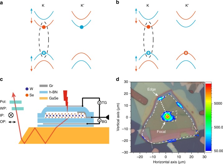
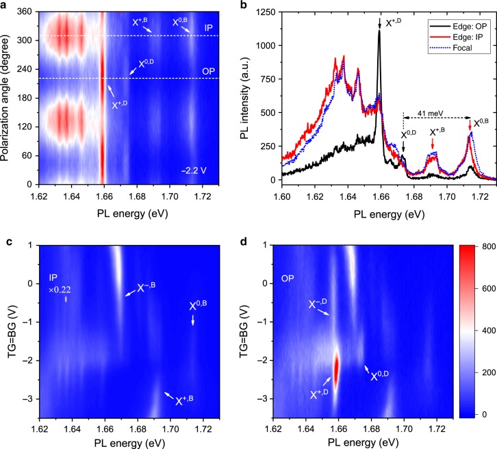
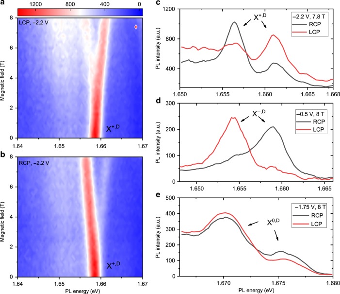
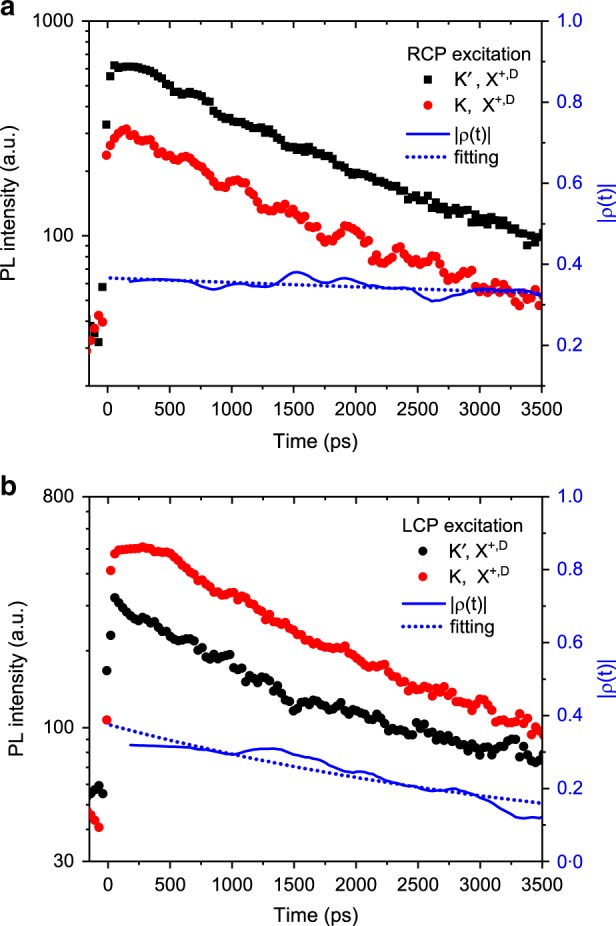
Single-layer transition metal dichalcogenides provide a promising material system to explore the electron's valley degree of freedom as a quantum information carrier. The valley degree of freedom can be directly accessed by means of optical excitation. However, rapid valley relaxation of optically excited electron-hole pairs (excitons) through the exchange interaction has been a major roadblock. Theoretically such valley relaxation is suppressed in dark excitons, suggesting a potential route for long valley lifetimes. Here we develop a waveguide-based method to detect time-resolved and energy-resolved dark exciton emission in single-layer WSe2, which involves spin-forbidden optical transitions with an out-of-plane dipole moment. The valley degree of freedom of dark excitons is accessed through the valley-dependent Zeeman effect under an out-of-plane magnetic field. We find a short valley lifetime for the dark neutral exciton, likely due to the short-range electron-hole exchange, but long valley lifetimes exceeding several nanoseconds for the dark charged excitons.
Conflict of interest statement
The authors declare no competing interests.
Figures
Similar articles
-
Probing dark excitons in atomically thin semiconductors via near-field coupling to surface plasmon polaritons.Nat Nanotechnol. 2017 Sep;12(9):856-860. doi: 10.1038/nnano.2017.106. Epub 2017 Jun 26. Nat Nanotechnol. 2017. PMID: 28650440
-
Optical initialization of a single spin-valley in charged WSe2 quantum dots.Nat Nanotechnol. 2019 May;14(5):426-431. doi: 10.1038/s41565-019-0394-1. Epub 2019 Mar 4. Nat Nanotechnol. 2019. PMID: 30833693
-
Up- and Down-Conversion between Intra- and Intervalley Excitons in Waveguide Coupled Monolayer WSe2.ACS Nano. 2020 Aug 25;14(8):10503-10509. doi: 10.1021/acsnano.0c04397. Epub 2020 Jul 22. ACS Nano. 2020. PMID: 32687318
-
Microsecond dark-exciton valley polarization memory in two-dimensional heterostructures.Nat Commun. 2018 Feb 21;9(1):753. doi: 10.1038/s41467-018-03174-3. Nat Commun. 2018. PMID: 29467477 Free PMC article.
-
Magnetic brightening and control of dark excitons in monolayer WSe2.Nat Nanotechnol. 2017 Sep;12(9):883-888. doi: 10.1038/nnano.2017.105. Epub 2017 Jun 26. Nat Nanotechnol. 2017. PMID: 28650442
Cited by
-
Strain control of hybridization between dark and localized excitons in a 2D semiconductor.Nat Commun. 2022 Dec 12;13(1):7691. doi: 10.1038/s41467-022-35352-9. Nat Commun. 2022. PMID: 36509779 Free PMC article.
-
Challenges and opportunities in 2D heterostructures for electronic and optoelectronic devices.iScience. 2022 Feb 19;25(3):103942. doi: 10.1016/j.isci.2022.103942. eCollection 2022 Mar 18. iScience. 2022. PMID: 35265814 Free PMC article. Review.
-
Enhanced Photo-excitation and Angular-Momentum Imprint of Gray Excitons in WSe2 Monolayers by Spin-Orbit-Coupled Vector Vortex Beams.ACS Nano. 2024 Apr 30;18(17):11425-11437. doi: 10.1021/acsnano.4c01881. Epub 2024 Apr 18. ACS Nano. 2024. PMID: 38637308 Free PMC article.
-
Ultralow Auger-Assisted Interlayer Exciton Annihilation in WS2/WSe2 Moiré Heterobilayers.Nano Lett. 2024 Mar 6;24(9):2773-2781. doi: 10.1021/acs.nanolett.3c04688. Epub 2024 Jan 29. Nano Lett. 2024. PMID: 38285707 Free PMC article.
-
Excitonic Complexes in Two-Dimensional Transition Metal Dichalcogenides.Nat Commun. 2023 Dec 12;14(1):8233. doi: 10.1038/s41467-023-44119-9. Nat Commun. 2023. PMID: 38086893 Free PMC article.
References
Grants and funding
LinkOut - more resources
Full Text Sources
Molecular Biology Databases
