

Exploring the reactivity of distinct electron transfer sites at CVD grown monolayer graphene through the selective electrodeposition of MoO2 nanowires
- PMID: 31492903
- PMCID: PMC6731215
- DOI: 10.1038/s41598-019-48022-6
Exploring the reactivity of distinct electron transfer sites at CVD grown monolayer graphene through the selective electrodeposition of MoO2 nanowires
Abstract
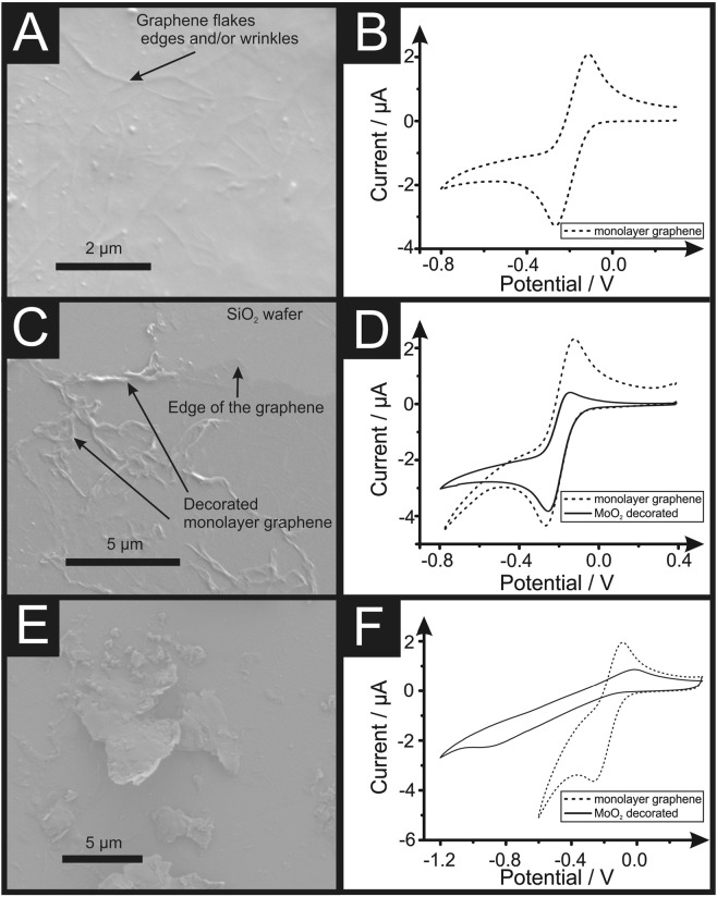
The origin of electron transfer at Chemical Vapour Deposition (CVD) grown monolayer graphene using a polymer-free transfer methodology is explored through the selective electrodeposition of Molybdenum (di)oxide (MoO2). The electrochemical decoration of CVD monolayer graphene with MoO2 is shown to originate from the edge plane like- sites/defects. Edge plane decoration of MoO2 nanowires upon monolayer graphene is observed via electrochemical deposition over short time periods only (ca. -0.6 V for 1 second (vs. Ag/AgCl)). At more electrochemically negative potentials (ca. -1.0 V) or longer deposition times, a large MoO2 film is created/deposited on the graphene sheet, originating and expanding from the original nucleation points at edge plane like- sites/defects/wrinkles. Nanowire fabrication along the edge plane like- sites/defects of graphene is confirmed with Cyclic Voltammetry, Scanning Electron Microscopy (SEM), Atomic Force Microscopy (AFM) and Raman Spectroscopy. Monitoring the electrochemical response towards [Ru(NH3)6]3+/2+ and comparing the heterogeneous electron transfer (HET) kinetics at CVD grown monolayer graphene prior and post nanowire fabrication reveals key understandings into the fundamental electrochemical properties of carbon materials. The HET kinetics ([Formula: see text]) at MoO2 nanowire decorated monolayer graphene sheets, when edge plane like- sites/defects have been coated/blocked with MoO2, are significantly reduced in comparison to the unmodified graphene alternative. Interestingly, MoO2 nucleation originates on the edge plane like- sites/defects of the graphene sheets, where the basal plane sites remain unaltered until the available edge plane like- sites/defects have been fully utilised; after which MoO2 deposition propagates towards and onto the basal planes, eventually covering the entire surface of the monolayer graphene surface. In such instances, there is no longer an observable electrochemical response. This work demonstrates the distinct electron transfer properties of edge and basal plane sites on CVD grown monolayer graphene, inferring favourable electrochemical reactivity at edge plane like- sites/defects and clarifying the origin of graphene electro-activity.
Conflict of interest statement
The authors declare no competing interests.
Figures

References
LinkOut - more resources
Full Text Sources
Miscellaneous
