. 2019 Sep 24;10(1):4334.
doi: 10.1038/s41467-019-12395-z.

Pen drawing display

Affiliations

Pen drawing display

Sang-Mi Jeong et al. Nat Commun. .

Abstract

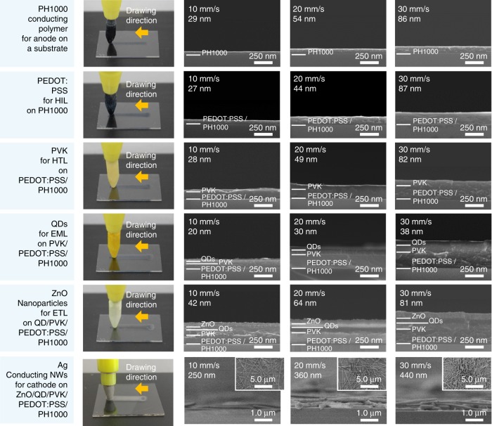
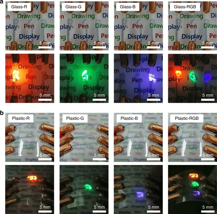
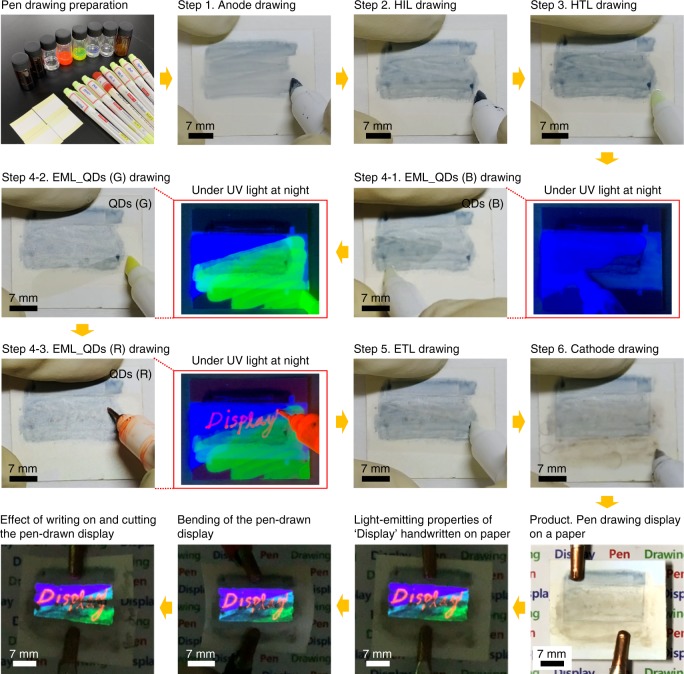
As advancements in science and technology, such as the Internet of things, smart home systems, and automobile displays, become increasingly embedded in daily life, there is a growing demand for displays with customized sizes and shapes. This study proposes a pen drawing display technology that can realize a boardless display in any form based on the user's preferences, without the usual restrictions of conventional frame manufacturing techniques. An advantage of the pen drawing method is that the entire complex fabrication process for the display is encapsulated in a pen. The display components, light-emitting layers, and electrodes are formed using felt-tip drawing pens that contain the required solutions and light-emitting materials. The morphology and thickness of each layer is manipulated by adjusting the drawing speed, number of drawing cycles, and substrate temperature. This study is expected to usher in the upcoming era of customized displays that can reflect individual user needs.


Conflict of interest statement

The authors declare no competing interests.

Figures

Fig. 1
Fig. 1
Pen-drawing display. a Schematic diagram of pen-drawing display with six drawing pens containing anode, hole injection layer (HIL), hole transfer layer (HTL), emission layer (EML), electron transfer layer (ETL), and cathode solutions. A quantum dot light-emitting diode (QD-LED) display fabricated using the pen-drawing method consists of PH1000 (anode), PEDOT:PSS (HIL), PVK (HTL), CdSeS@ZnS (red (R), EML), CdZnSeS@ZnS (green (G), EML), CdZnS@ZnS (blue (B), EML), zinc oxide nanoparticles (ZnO NPs, ETL), and silver nanowires (Ag NWs, cathode). b Optical image (left) of the pen-drawing apparatus setup. The pen drawing was performed using a custom-built three-axis micropositioning system controlled by a computer-programmable motion controller. Field emission scanning electron microscopy (FE-SEM) image (right) of the pen point of the felt-tip pen. c Schematic diagram and working principle of film formation through pen drawing
Fig. 2
Fig. 2
Gallery of pen-drawing images. PH1000, PEDOT:PSS, poly(N-vinylcarbazole) (PVK), QDs, ZnO NPs, and Ag NWs were deposited in order, and the thickness of each layer was observed using FE-SEM. The nanometer-scale thickness could be controlled by manipulating the drawing speed while the number of drawing cycles (1 half-cycle) and substrate temperature (20 °C) were fixed
Fig. 3
Fig. 3
Electrical and optical properties of PH1000 and Ag NWs. Sheet resistance, optical transmittance, and photo images of PH1000 (a) and Ag NWs (b) depending on the number of drawing cycles. c Transmittance when each layer (PH1000, PEDOT:PSS, PVK, QDs, ZnO NPs, and Ag NWs) is sequentially formed on a glass substrate
Fig. 4
Fig. 4
Surface morphology of each layer formed by pen drawing. Atomic force microscopy (AFM) topographic images, height section analyses, and three-dimensional images of PH1000 (a), PEDOT:PSS (b), PVK (c), QDs for G (d), ZnO (e), and Ag NWs (f)
Fig. 5
Fig. 5
Luminance–current–voltage (LIV) characteristics of the QD light-emitting diodes (QD-LEDs) fabricated using the pen-drawing method. Energy levels of red (R), green (G), and blue (B) QD-LEDs. Highest occupied molecular orbital (HOMO) and lowest unoccupied molecular orbital (LUMO) levels of PH1000, PEDOT:PSS, PVK, QDs, ZnO NPs, and Ag NWs. CdSeS@ZnS for R emission (a); CdZnSeS@ZnS for G emission (b); and CdZnS@ZnS for B emission (c). Luminance (d), efficiency (e), and electroluminescence spectra and the Commission Internationale de l'Elcairage (CIE) color coordinates (f) corresponding to the R, G, and B emitting QD-LEDs with the structure of PH1000/PEDOT:PSS/PVK/QDs (CdSeS@ZnS for R, CdZnSeS@ZnS for G, and CdZnS@ZnS for B)/ZnO NPs/Ag NWs
Fig. 6
Fig. 6
Handwriting display images using the pen-drawing method. Photo images of “RGB” text displays formed on the glass (a) and plastic (b) substrates, showing the optical clarity and mechanical flexibility
Fig. 7
Fig. 7
Handwriting images using the pen-drawing method. Photo images of “Display” handwritten on paper, showing the light-emitting ability, mechanical flexibility, and tearing properties

References

    1. Park S-I, et al. Printed assemblies of inorganic light-emitting diodes for deformable and semitransparent displays. Science. 2009;325:977–981. doi: 10.1126/science.1175690. - DOI - PubMed
    1. Kim T-H, et al. Full-colour quantum dot displays fabricated by transfer printing. Nat. Photonics. 2011;5:176. doi: 10.1038/nphoton.2011.12. - DOI
    1. Choi MK, et al. Wearable red–green–blue quantum dot light-emitting diode array using high-resolution intaglio transfer printing. Nat. Commun. 2015;6:7149. doi: 10.1038/ncomms8149. - DOI - PMC - PubMed
    1. Zheng H, et al. All-solution processed polymer light-emitting diode displays. Nat. Commun. 2013;4:1971. doi: 10.1038/ncomms2971. - DOI - PubMed
    1. Pardo DA, Jabbour GE, Peyghambarian N. Application of screen printing in the fabrication of organic light-emitting devices. Adv. Mater. 2000;12:1249–1252. doi: 10.1002/1521-4095(200009)12:17<1249::AID-ADMA1249>3.0.CO;2-Y. - DOI

Publication types