

Improved Memory Properties of Graphene Oxide-Based Organic Memory Transistors
- PMID: 31557870
- PMCID: PMC6843658
- DOI: 10.3390/mi10100643
Improved Memory Properties of Graphene Oxide-Based Organic Memory Transistors
Abstract
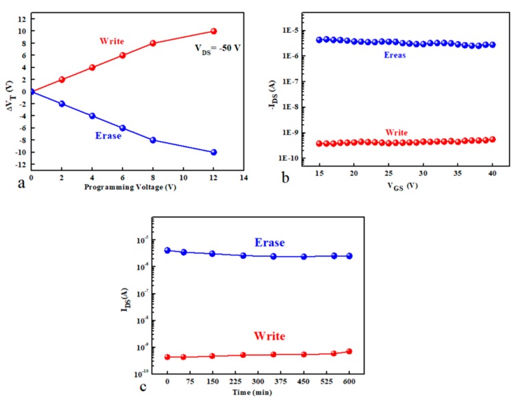
To investigate the behaviour of the organic memory transistors, graphene oxide (GO) was utilized as the floating gate in 6,13-Bis(triisopropylsilylethynyl)pentacene (TIPS-pentacene)-based organic memory transistors. A cross-linked, off-centre spin-coated and ozone-treated poly(methyl methacrylate) (cPMMA) was used as the insulating layer. High mobility and negligible hysteresis with very clear transistor behaviour were observed for the control transistors. On the other hand, memory transistors exhibited clear large hysteresis which is increased with increasing programming voltage. The shifts in the threshold voltage of the transfer characteristics as well as the hysteresis in the output characteristics were attributed to the charging and discharging of the floating gate. The counter-clockwise direction of hysteresis indicates that the process of charging and discharging the floating gate take place through the semiconductor/insulator interface. A clear shift in the threshold voltage was observed when different voltage pulses were applied to the gate. The non-volatile behaviour of the memory transistors was investigated in terms of charge retention. The memory transistors exhibited a large memory window (~30 V), and high charge density of (9.15 × 1011 cm-2).
Keywords: 6,13-Bis(triisopropylsilylethynyl)pentacene (TIPS-pentacene); cross-linked poly(methyl methacrylate) PMMA; graphene oxide; organic memory transistors.
Conflict of interest statement
The authors declare no conflict of interest.
Figures


References
-
- Baeg K.J., Noh Y.Y., Sirringhaus H., Kim Y.K. Controllable shifts in threshold voltage of top-gate polymer field-effect transistors for applications in organic nano floating gate memory. Adv. Funct. Mater. 2010;20:224. doi: 10.1002/adfm.200901677. - DOI
-
- Han J., Wang W., Ying J., Xie W. Ambipolar organic thin-film transistor-based nano-floating-gate nonvolatile memory. Appl. Phys. Lett. 2014;104:013302. doi: 10.1063/1.4860990. - DOI
-
- Baeg K.J., Noh Y.Y., Ghim J., Kang S.J., Lee H., Kim D.Y. Organic nonvolatile memory based on pentacene field-effect transistors using a polymeric gate electret. Adv Mater. 2006;18:3179. doi: 10.1002/adma.200601434. - DOI
-
- Guo Y., Yu G., Liu Y.Q., Guo Y.L., Di C.A., Ye S.H., Sun X.N., Zheng J., Wen Y.G., Wu W.P. Multibit storage of organic thin-film field-effect transistors. Adv. Mater. 2009;21:1954. doi: 10.1002/adma.200802430. - DOI
LinkOut - more resources
Full Text Sources
Miscellaneous
