. 2019 Sep 30;10(1):4279.
doi: 10.1038/s41467-019-12196-4.

Broadband transparent optical phase change materials for high-performance nonvolatile photonics

Affiliations

Broadband transparent optical phase change materials for high-performance nonvolatile photonics

Yifei Zhang et al. Nat Commun. .

Abstract

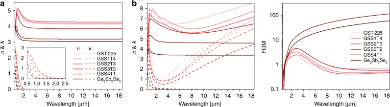
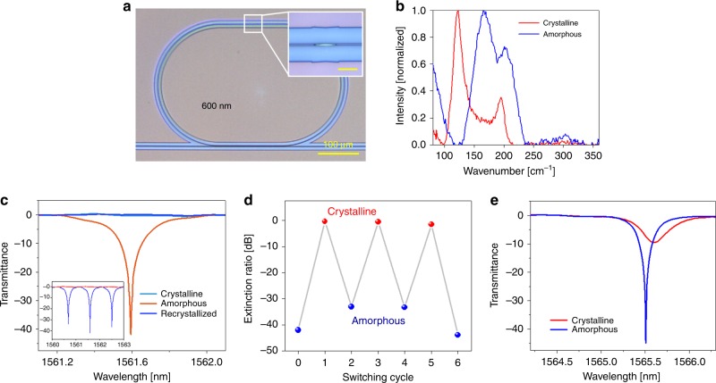
Optical phase change materials (O-PCMs), a unique group of materials featuring exceptional optical property contrast upon a solid-state phase transition, have found widespread adoption in photonic applications such as switches, routers and reconfigurable meta-optics. Current O-PCMs, such as Ge-Sb-Te (GST), exhibit large contrast of both refractive index (Δn) and optical loss (Δk), simultaneously. The coupling of both optical properties fundamentally limits the performance of many applications. Here we introduce a new class of O-PCMs based on Ge-Sb-Se-Te (GSST) which breaks this traditional coupling. The optimized alloy, Ge2Sb2Se4Te1, combines broadband transparency (1-18.5 μm), large optical contrast (Δn = 2.0), and significantly improved glass forming ability, enabling an entirely new range of infrared and thermal photonic devices. We further demonstrate nonvolatile integrated optical switches with record low loss and large contrast ratio and an electrically-addressed spatial light modulator pixel, thereby validating its promise as a material for scalable nonvolatile photonics.


Conflict of interest statement

The authors declare no competing interests.

Figures

Fig. 1
Fig. 1
Impact of Se substitution revealed by density functional theory (DFT) simulations. Atomic structures of a hexagonal Ge2Sb2Se4Te1 (GSS4T1); b cubic GSS4T1; and c orthorhombic Ge2Sb2Se5 with the representative atomic blocks highlighted by the yellow shaded areas. Unit cells, loosely bound Te/Se double layers, and aggregated vacancies are presented by the black boxes, dashed rectangle, and dashed circles, respectively. d Cohesive energies of the cubic and orthorhombic phases relative to their hexagonal counterparts with various Se concentrations
Fig. 2
Fig. 2
Comparison of electronic structures of hexagonal and orthorhombic phases. a DOS of hexagonal Ge–Sb–Se–Te and orthorhombic Ge2Sb2Se5, with the Fermi level illustrated by the dashed line. Band structures of b hexagonal Ge2Sb2Se4Te1 (GSS4T1); and c orthorhombic Ge2Sb2Se5. Charge densities of d, f valence band maximum (VBM) in blue and e, g conduction band minimum (CBM) in magenta of d, e hexagonal GSS4T1 and f, g orthorhombic Ge2Sb2Se5
Fig. 3
Fig. 3
In-situ TEM analysis of the crystallization process of Ge2Sb2Se4Te1 (GSS4T1). a Low-magnification and b higher-magnification images of GSS4T1 film on a SiN holder after heating at 400 °C for 5 min. c Local fast Fourier transformation (FFT) of b showing two sets of reciprocal lattice points, which reveals that the sample contains two sets of hexagonal reflexes with a twist angle. d High-magnification image of the film after further annealing at 500 °C for 10 min. FFT analysis of the yellow square region shown in the inset indicates absence of the rotational stacking fault observed in b. e A back-folded region of the film suspending over a hole in the SiN support (corresponding to the red rectangle in the inset), where the layered structure of hexagonal GSS4T1 is evident
Fig. 4
Fig. 4
Electronic properties of Ge2Sb2SexTe5−x alloys. a Temperature dependence of resistivity of Ge2Sb2Te5, Ge2Sb2Se2Te3, and Ge2Sb2Se4Te1 (GSS4T1) upon annealing: the distinct drop marked by blue dotted lines correspond to crystallization of the amorphous phase to the metastable cubic phase, whereas the green dotted line labels the transition towards the stable hexagonal phase. b Hall conductivity, c hole concentration, and d Hall mobility of c-Ge2Sb2SexTe5−x; for all compositions, the films were annealed 50 °C above the amorphous-to-cubic transition temperature. e Temperature-dependent resistivity of GSS4T1 annealed at different three temperatures: 265, 340, and 383 °C. The temperature coefficients of resistivity are negative in all cases evidenced by the negative slope of the cooling curves
Fig. 5
Fig. 5
Optical properties of Ge2Sb2SexTe5-x films. a, b Measured real (n) and imaginary (k) parts of refractive indices of the a amorphous and b crystalline alloys. c Material FOM’s
Fig. 6
Fig. 6
Non-volatile integrated photonic switches based on optical phase change materials (O-PCMs). a Optical micrograph of the resonant switch: inset shows the Ge2Sb2Se4Te1 (GSS4T1) strip on top of the SiN waveguide. b Raman spectra of laser switched GSS4T1, where the peaks at 160 and 120 cm−1 are signatures of the amorphous and crystalline states, respectively. c Normalized transmittance spectra of the resonant switch integrated with GSS4T1, showing complete on/off modulation of the resonant peaks. Inset displays the broadband transmittance spectra of the same device. The three spectra correspond to three states of GSS4T1: (orange) as-deposited amorphous, (light blue) crystallized through furnace annealing, and (blue) laser recrystallized. d Resonance extinction ratio modulation of the device upon laser switching. e Normalized transmittance spectra of a reference switch device integrated with Ge2Sb2Te5
Fig. 7
Fig. 7
Electrothermal switching of Ge2Sb2Se4Te1 (GSS4T1). a Schematic of the device and test setup. b Top-view optical micrograph of the full device used to switch a 10 μm × 10 μm pixel. The three contact pads were used ground-source-ground electrical contacts. Scale bar: 100 μm. c Zoom-in on the pixel with a square pattern of GSS4T1. d Time-dependent absolute reflection measurements of a 1550 nm laser focused onto the pixel. e Raman measurements of the GSS4T1 film after an electrical amorphization and crystallization pulse profile

References

    1. Wuttig M, Bhaskaran H, Taubner T. Phase-change materials for non-volatile photonic applications. Nat. Photonics. 2017;11:465–476. doi: 10.1038/nphoton.2017.126. - DOI
    1. Stegmaier M, Ríos C, Bhaskaran H, Wright CD, Pernice WH. Nonvolatile all‐optical 1 × 2 switch for chipscale photonic networks. Adv. Optical Mater. 2017;5:1600346. doi: 10.1002/adom.201600346. - DOI
    1. Rudé M, et al. Optical switching at 1.55 μm in silicon racetrack resonators using phase change materials. Appl. Phys. Lett. 2013;103:141119. doi: 10.1063/1.4824714. - DOI
    1. Moriyama T, et al. Ultra-compact, self-holding asymmetric Mach-Zehnder interferometer switch using Ge2Sb2Te5 phase-change material. IEICE Electron. Express. 2014;11:20140538. doi: 10.1587/elex.11.20140538. - DOI
    1. Kato K, Kuwahara M, Kawashima H, Tsuruoka T, Tsuda H. Current-driven phase-change optical gate switch using indium–tin-oxide heater. Appl. Phys. Express. 2017;10:072201. doi: 10.7567/APEX.10.072201. - DOI

Publication types