. 2019 Oct 10;9(1):14618.
doi: 10.1038/s41598-019-51039-6.

Stateful Three-Input Logic with Memristive Switches

Affiliations

Stateful Three-Input Logic with Memristive Switches

A Siemon et al. Sci Rep. .

Abstract

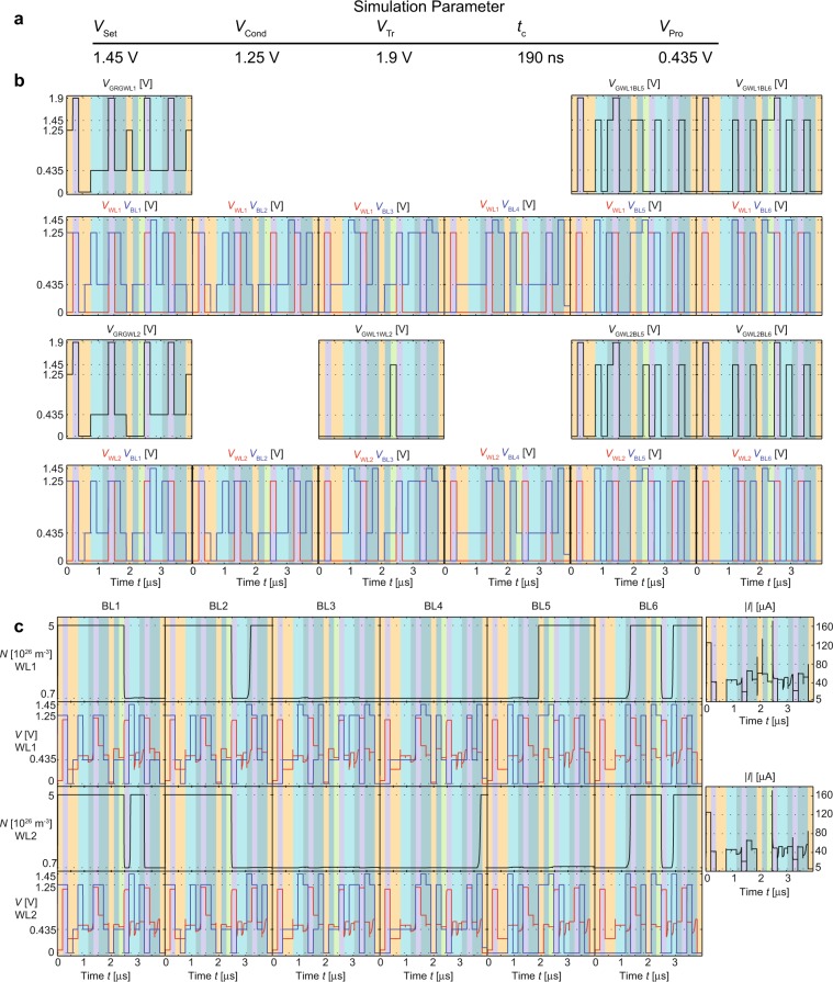
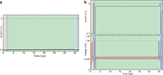
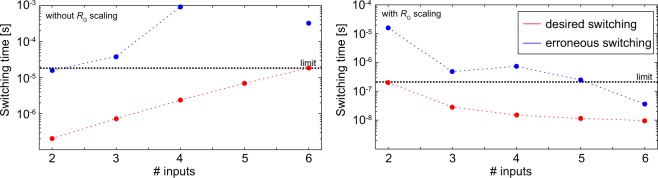
Memristive switches are able to act as both storage and computing elements, which make them an excellent candidate for beyond-CMOS computing. In this paper, multi-input memristive switch logic is proposed, which enables the function X OR (Y NOR Z) to be performed in a single-step with three memristive switches. This ORNOR logic gate increases the capabilities of memristive switches, improving the overall system efficiency of a memristive switch-based computing architecture. Additionally, a computing system architecture and clocking scheme are proposed to further utilize memristive switching for computation. The system architecture is based on a design where multiple computational function blocks are interconnected and controlled by a master clock that synchronizes system data processing and transfer. The clocking steps to perform a full adder with the ORNOR gate are presented along with simulation results using a physics-based model. The full adder function block is integrated into the system architecture to realize a 64-bit full adder, which is also demonstrated through simulation.


Conflict of interest statement

The authors declare no competing interests.

Figures

Figure 1
Figure 1
The ORNOR gate’s (a) structure and (b) truth table. (c) Simulation parameter for the circuit of (a). (d) The simulation of the critical cases of the ORNOR gate are depicted. Here, the subscripts X, Y, Z are indicating the correlation of the applied voltages, currents or state variables to the devices X, Y and Z, respectively. In step 1–3 the initialization process of the ORNOR gate is shown by writing the three inputs to the devices X (blue), Y (light green) and Z (yellow). In step 4 (red) the ORNOR operation is executed, which is followed by three verifying read-out steps (dark green). If a high current is detected the read-out value is a 1, whereas a low current is a 0. Row 1/2/3: voltage applied to the Bitline 2/Bitline 1/Bitline 0. Row 4: potential at the wordline. Row 5/6/7: current at Bitline 2/Bitline 1/Bitline 0. Row 8/9/10: state variable of device X/Y/Z. The scale is changed for small state variable values.
Figure 2
Figure 2
Computing architecture for a memristive computing system. (a) The computing system architecture utilizes a synchronized, interconnected array of function blocks to perform complex functions with improved efficiency. Each function block contains a set of memristive switches, which, in conjunction with a set of clock signals, perform a predefined function. For complex computations the data can be processed in multiple function blocks. The transfer between function blocks is done with the data transfer transistor. (b) An optimized full adder schematic with six total memristive switches. The signals, which need to be applied for a FALSE operation of device AWL1, are displayed in violet. (c) Two-Bit adder circuit with parasitic elements. RP and CP are the parasitic resistors and the parasitic capacitances of the wordlines and bitlines. Here the parasitic capacitances between the wordlines are not depicted due to readability. The signals, which need to be applied for a COPY operation from device C1WL1 to C0WL2, are displayed in green.
Figure 3
Figure 3
Clocking scheme for a full adder. Each line corresponds to a step in the full adder, with the exception of simulation requirements for loading and transferring data (marked by–). Each step provides the operation that is performed, including the memristive switches that are part of the computation. The result of the operation is shown for each memristive switch, and if there is no value in a cell, it is assumed that the memristive switch maintains its previous state. SET operations are yellow, FALSE operations are violet, COPY operations are light green, IMP operations are green and ORNOR operations are dark green.
Figure 4
Figure 4
(a) Independent clocking and (b) parallel clocking scheme. (a) In the independent clocking scheme, each functional block has an independent set of clocks, which can be applied at any time to perform the function. In this way, each functional block is aligned so that there is no idle time, however, an increased number of clocks and drivers are required. Approach (b) uses the same set of clock signals to drive all memristive switches for the multi-bit addition. The first eight steps and last seven steps are driven across all function blocks simultaneously. This approach is able to compute the multi-bit full addition in the same number of steps while significantly reducing the number of clock signals required due to parallel control of multiple function blocks.
Figure 5
Figure 5
Simulation of a one-bit full adder. (a) Circuit parameter. (b) Applied voltages. SET processes are yellow, RESET operations are violet COPY operations are light green, IMP operations green and ORNOR operations dark green. Row 1/3: voltage applied to the load transistor and voltages applied to the selecting transistors of WL1/2. Additional in row 3: voltage transient applied to the data transfer gate, which can connect WL1 and WL2. Row 2/4: voltages applied to the bitlines (blue) and the wordlines (red) WL1/WL2. The circuit parameter voltages are marked for better readability. (c) State variables and terminal voltages of the one-bit adder. Row 1/3: transient of the state variable and wordline current of WL1/WL2. Row 2/4: wordline potential (red) of WL1/WL2 and voltages applied to the bitline (blue) of each device.
Figure 6
Figure 6
Simulation and comparison of the multibit adder. (a) State variable of SWL65 under the worst case conditions. The worst case is found to be A – B, where A is 0 and B is 0. The color scheme is adopted from Fig. 3. (b) State variable and applied voltage of M1WL65 for the worst case simulation. The potential of the wordline is depicted in red and the potential of the connection point at the bitline is shown in blue.
Figure 7
Figure 7
Simulation of the two multi-input approaches with (left) and without (right) RG scaling. In both plots, two switching times of the device connected to VSet are depicted. In the red case, all devices are in the HRS, and the proper desired functionality is that the device should switch (desired switching). The blue points depicts the switching time if one of the devices connected to VCond is in the LRS. In this case, the device should not switch (erroneous switching). The limit is chosen as the slowest of the desired switching processes; all erroneous switching processes must be slower than this limit.

References

    1. Frank D, et al. Device scaling limits of Si MOSFETs and their application dependencies. Proceedings of the IEEE. 2001;89:259–288. doi: 10.1109/5.915374. - DOI
    1. Williams RS. What’s Next? [The end of Moore’s law] Computing in Science & Engineering. 2017;19:7–13. doi: 10.1109/MCSE.2017.31. - DOI
    1. ITRS, International Technology Roadmap for Semiconductors 2.0 - 2015 Edition (2015).
    1. Wong H-SP, Salahuddin S. Memory leads the way to better computing. Nat. Nanotechnol. 2015;10:191–194. doi: 10.1038/nnano.2015.29. - DOI - PubMed
    1. Kautz W. Cellular Logic-in-Memory Arrays. IEEE Transactions on Computers C. 1969;18:719–727. doi: 10.1109/T-C.1969.222754. - DOI