Review
. 2019 Oct 11;9(4):121.
doi: 10.3390/bios9040121.

Polarization Induced Electro-Functionalization of Pore Walls: A Contactless Technology

Affiliations
Review

Polarization Induced Electro-Functionalization of Pore Walls: A Contactless Technology

Aurélie Bouchet-Spinelli et al. Biosensors (Basel). .

Abstract

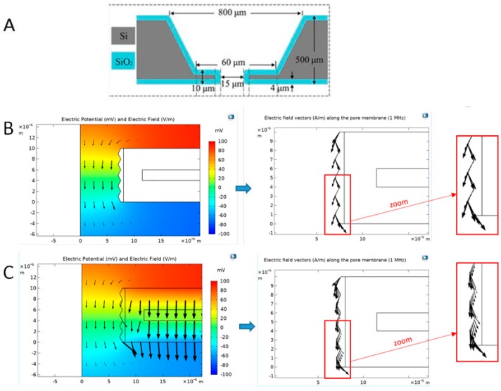
This review summarizes recent advances in micro- and nanopore technologies with a focus on the functionalization of pores using a promising method named contactless electro-functionalization (CLEF). CLEF enables the localized grafting of electroactive entities onto the inner wall of a micro- or nano-sized pore in a solid-state silicon/silicon oxide membrane. A voltage or electrical current applied across the pore induces the surface functionalization by electroactive entities exclusively on the inside pore wall, which is a significant improvement over existing methods. CLEF's mechanism is based on the polarization of a sandwich-like silicon/silicon oxide membrane, creating electronic pathways between the core silicon and the electrolyte. Correlation between numerical simulations and experiments have validated this hypothesis. CLEF-induced micro- and nanopores functionalized with antibodies or oligonucleotides were successfully used for the detection and identification of cells and are promising sensitive biosensors. This technology could soon be successfully applied to planar configurations of pores, such as restrictions in microfluidic channels.

Keywords: CLEF; biosensing; contactless; electro-functionalization; micropore; nanopore.


Conflict of interest statement

The authors declare no conflict of interest.

Figures

Scheme 1
Scheme 1
Target detection principle with a single pore. (A) Translocation of a biomolecule in a dielectric membrane. (B) Current decrease caused by the transit of biomolecules.
Figure 1
Figure 1
Implementation of contactless electro-functionalization (CLEF). (A) Principle of the specific functionalization of the inner wall of the pore. SEM characterizations of (B) naked pore, (C) iridium oxide deposit, (D) gold deposit, (E) oligonucleotide-functionalized polypyrrole (PPy-ODN) deposit also revealed using fluorescence microscopy (F).
Figure 2
Figure 2
Distribution of the electric field in a micrometric pore made in a silica-covered silicon membrane. (A) Schematic side-view of a 15 µm-wide micropore. (B) Numerical simulation of a perfectly insulated pore membrane immersed in a 100 mM KCl solution in contact with two Ag/AgCl electrodes at applied potentials +100 mV (top electrode) and −100 mV (bottom electrode). (Left) The complete potential drop is confined inside the pore at 1 MHz (colors). Vectors (black) represent the resulting electric field distribution. (Right) Electric field vectors along the pore membrane boundary: As expected, the electric field is tangential to the membrane surface. (C) Numerical simulation taking into account the dielectric properties of the pore membrane (Si covered by a 4 µm-thick SiO2 layer). (Left) The SiO2 layer of the pore membrane is highly polarized as it experiences the complete drop of the applied potential (+100 to −100 mV). (Right) Electric field vectors along the pore membrane boundary: The electric field displays a non-zero component normal to the membrane surface.
Figure 3
Figure 3
Validation of the numerical model by comparing measured impedances (continuous lines) against computed impedances (dashed lines) for different KCl solutions. (A) Bode plots of impedance norm. (B) Bode plots of impedance phase.
Figure 4
Figure 4
Evidences for the influence of the core silicon on CLEF deposition. (A) Computed impedance phases of the sandwich-like membranes without any core silicon layer (red line) or with various thicknesses of the core silicon layer (blue, green, and dashed lines are overlapped). (B) Fluorescence revelation of the deposition of PPy-ODNs in micropores. SEM pictures of gold nanobead deposits using current intensities of (C) 2 µA, (D) 5 µA, and (E) 11 µA.
Figure 5
Figure 5
Correlation between numerical simulation and experimental data when analyzing the influence of the pore geometry. (A) Numerical simulation (radial electrical field, Er) showing the polarization of one side of the pore membrane. (B,C) The side of gold deposition could be controlled experimentally by achieving (B) electro-oxidation or (C) electro-reduction.
Figure 6
Figure 6
Different morphologies for gold deposition according to (A) current or (B) voltage applications in the CLEF protocol.
Figure 7
Figure 7
Functionalized nanopore sensing of oligodesoxyribonucleotide (ODN)-coated nanoparticles. (A) A nanopore electro-functionalized with oligonucleotides via CLEF was employed for the detection of gold nanoparticles carrying complementary (red) or non-complementary (black) ODNs. (B) SEM characterization of (a) functionalized or (b) non-functionalized nanopores. (C) Electrosensing. The current, measured via platinum electrodes, distinguishes the passage of complementary and non-complementary targets in the ODN-electro-functionalized nanopore.
Figure 8
Figure 8
Typical current versus time traces of ODN-coated polystyrene (PS) particles passing through an ODN-functionalized micropore. (A) Translocation of non-complementary (nc)-ODN-PS. (B) Capture of complementary (c)-ODN-PS.
Figure 9
Figure 9
Selective capture of B- or T-lymphocytes using CLEF specific antibody-functionalized micropores. T-lymphocytes were selectively fluorescently labeled for visualization purposes. (A) Schematic principle of micropore functionalization strategy. (B) Transmission and fluorescence microscopy images of cells captured in antibody-functionalized micropores and stacks of the images. The white dashed circles in the fluorescence images indicate the position of the micropore wall.
Figure 10
Figure 10
(A) Schematic principle of the silicon micropore with a deoxidized region (green) and Au feeder electrodes. Inset: simultaneous reduction of water at the cathodically polarized region (yellow) and oxidation of electrochemiluminescent (ECL) reagents at the anodically polarized region (red), leading to ECL light emission in the micropore. (B) SEM images of the p-doped silicon microchip with the solid-state micropore and the integrated feeder Au electrodes. The deoxidized regions appear darker around the micropore. Pore dimensions: 20 µm (length) × 10 µm (width) × 20 µm (height). (C) Photoluminescent (a), ECL (b), and overlay (c) of both luminescence images of the same region of interest around the micropore. Both axes are represented and the origin, O, of the axes is defined as the center of the micropore. The dashed lines materialize the micropore walls.

References

    1. Wanunu M. Nanopores: A journey towards DNA sequencing. Phys. Life Rev. 2012;9:125–158. doi: 10.1016/j.plrev.2012.05.010. - DOI - PMC - PubMed
    1. Varongchayakul N., Song J., Meller A., Grinstaff M.W. Single-molecule protein sensing in a nanopore: A tutorial. Chem. Soc. Rev. 2018;47:8512–8524. doi: 10.1039/C8CS00106E. - DOI - PMC - PubMed
    1. Dekker C. Solid-state nanopores. Nat. Nanotechnol. 2007;2:209–215. doi: 10.1038/nnano.2007.27. - DOI - PubMed
    1. Branton D., Deamer D.W., Marziali A., Bayley H., Benner S.A., Butler T., Di Ventra M., Garaj S., Hibbs A., Huang X., et al. The potential and challenges of nanopore sequencing. Nat. Biotechnol. 2008;26:1146–1153. doi: 10.1038/nbt.1495. - DOI - PMC - PubMed
    1. Deamer D., Akeson M., Branton D. Three decades of nanopore sequencing. Nat. Biotechnol. 2016;34:518–524. doi: 10.1038/nbt.3423. - DOI - PMC - PubMed

LinkOut - more resources