. 2019 Nov 8;5(11):eaaw5593.
doi: 10.1126/sciadv.aaw5593. eCollection 2019 Nov.

Room temperature strain-induced Landau levels in graphene on a wafer-scale platform

Affiliations

Room temperature strain-induced Landau levels in graphene on a wafer-scale platform

P Nigge et al. Sci Adv. .

Abstract

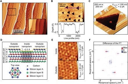
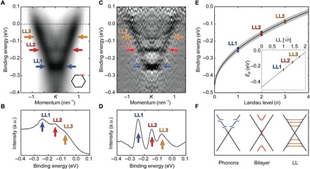
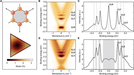
Graphene is a powerful playground for studying a plethora of quantum phenomena. One of the remarkable properties of graphene arises when it is strained in particular geometries and the electrons behave as if they were under the influence of a magnetic field. Previously, these strain-induced pseudomagnetic fields have been explored on the nano- and micrometer-scale using scanning probe and transport measurements. Heteroepitaxial strain, in contrast, is a wafer-scale engineering method. Here, we show that pseudomagnetic fields can be generated in graphene through wafer-scale epitaxial growth. Shallow triangular nanoprisms in the SiC substrate generate strain-induced uniform fields of 41 T, enabling the observation of strain-induced Landau levels at room temperature, as detected by angle-resolved photoemission spectroscopy, and confirmed by model calculations and scanning tunneling microscopy measurements. Our work demonstrates the feasibility of exploiting strain-induced quantum phases in two-dimensional Dirac materials on a wafer-scale platform, opening the field to new applications.


Figures

Fig. 1
Fig. 1. Identification of strained nanoprisms.
(A) Horizontal derivative AFM topography image of our monolayer graphene grown on a SiC substrate. Triangular nanoprisms are dispersed on the surface. Inset: AFM topography image of the same area. Substrate terrace steps are approximately 10 nm in height. (B) Top: Close-up view of AFM topography of the area indicated by the black box in (A). Bottom: Line cut through the AFM data marked by the purple line in the close-up view. (C) Overview STM topography image (200 nm × 200 nm, Vsample = 100 mV, Itun. = 2 pA) showing a single nanoprism. (D) Schematic structure of 6H-SiC showing its layered ABCACB stacking order with epitaxial graphene on top (yellow). Inside the nanoprism, a single layer within the unit cell is missing, exposing the graphene to a different substrate surface termination, as illustrated in the top view. The carbon buffer layer is not shown for clarity. (E) Atomically resolved STM images (10 nm × 10 nm, Vsample = 30 mV, Itun. = 2 pA) inside (top) and outside (bottom) of the nanoprism. (F) Difference map of the two Fourier transformed (FT) images in (E) visualizing the strain pattern inside the nanoprism.
Fig. 2
Fig. 2. Momentum-resolved visualization of LLs.
(A) ARPES cut through the Dirac cone at the K point at 300 K. The data have been divided by the Fermi function and symmetrized to compensate for matrix element effects (48). (B) Cut along the energy axis integrated around the K point in (A) in arbitrary units (a.u.). (C) Second derivative of the data in (A) (49). (D) Inverted second derivative of the data shown in (B) after smoothing. (A to D) LLs are indicated by arrows. (E) Summary of LL datasets, with model fit according to Eq. 1 shown in black; the 95% confidence interval of the fit is shown in gray. Different symbols indicate different samples and temperatures: sample A (6 K; hexagons), sample B (6 K; squares), sample B second dataset (6 K; stars), sample B (300 K; diamonds), sample C (6 K; circles), and sample C second dataset (6 K; triangles). ARPES data for the additional samples can be found in fig. S7. Inset: Same data plotted versus n, giving the expected linear behavior for LLs in a Dirac material. (F) Sketch of various mechanisms that may lead to ARPES intensity inside the cone. Neither electron-phonon coupling nor contamination from bilayer graphene can explain the experimental findings.
Fig. 3
Fig. 3. Model calculation of strain-induced LLs.
(A) Top: Honeycomb lattice, with the two sublattices A (red) and B (yellow). The black arrows indicate the symmetry of the strain pattern. Bottom: Triangular flake with strain-induced pseudomagnetic field B = 41 T. The color scale indicates the relative bond stretching. (B) Spectral function for the gapless case with Semenoff mass M = 0 meV. (C) Energy cut through the Dirac point (K) of the spectral function in (B). The dashed gray lines indicate the position of the LLs predicted by Eq. 1. (D) Spectral function averaged over a uniform distribution of Semenoff masses M ∈ [−135,135] meV. (E) Energy cut through the Dirac point (K) of the spectral function in (D). The shaded gray area indicates the broadening of the LLs predicted by Eqs. 1 and 2.

References

    1. Novoselov K. S., Jiang D., Schedin F., Booth T. J., Khotkevich V. V., Morozov S. V., Geim A. K., Two-dimensional atomic crystals. Proc. Natl. Acad. Sci. U.S.A. 102, 10451–10453 (2005). - PMC - PubMed
    1. Geim A. K., Novoselov K. S., The rise of graphene. Nat. Mater. 6, 183–191 (2007). - PubMed
    1. Castro Neto A. H., Guinea F., Peres N. M. R., Novoselov K. S., Geim A. K., The electronic properties of graphene. Rev. Mod. Phys. 81, 109–162 (2009).
    1. Anderson M. H., Ensher J. R., Matthews M. R., Wieman C. E., Cornell E. A., Observation of bose-einstein condensation in a dilute atomic vapor. Science 269, 198–201 (1995). - PubMed
    1. Osheroff D. D., Richardson R. C., Lee D. M., Evidence for a new phase of solid He3. Phys. Rev. Lett. 28, 885–888 (1972).

Publication types