Review
. 2019 Dec 9;10(1):5625.
doi: 10.1038/s41467-019-13332-w.

Quantum nanophotonics with group IV defects in diamond

Affiliations
Review

Quantum nanophotonics with group IV defects in diamond

Carlo Bradac et al. Nat Commun. .

Erratum in

Abstract

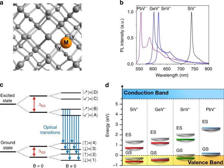
Diamond photonics is an ever-growing field of research driven by the prospects of harnessing diamond and its colour centres as suitable hardware for solid-state quantum applications. The last two decades have seen the field shaped by the nitrogen-vacancy (NV) centre with both breakthrough fundamental physics demonstrations and practical realizations. Recently however, an entire suite of other diamond defects has emerged-group IV colour centres-namely the Si-, Ge-, Sn- and Pb-vacancies. In this perspective, we highlight the leading techniques for engineering and characterizing these diamond defects, discuss the current state-of-the-art group IV-based devices and provide an outlook of the future directions the field is taking towards the realisation of solid-state quantum photonics with diamond.


Conflict of interest statement

The authors declare no competing interests.

Figures

Fig. 1
Fig. 1
Photoluminescence of group IV centres in diamond. a Atomic structure of group IV colour centres in the D3d symmetry, split-vacancy configuration. The group IV element (M, orange) lies between two nearest-neighbours missing carbon atoms (V, white). b Typical room temperature photoluminescence (PL) spectrum of SiV, GeV, SnV and PbV centres. c Energy structure of impurity-divacancy centres within zero and non-zero external magnetic field B. d Predicted energies of the ground (GS) and excited (ES) states of the group IV colour centres with respect to the diamond valence band maximum (i.e. the location of the valence band at the Brillouin-zone centre). Levels in grey, red, green and blue refer to values calculated in refs. ,,,.
Fig. 2
Fig. 2
Coherent spin control in the SiV centre. a Spin control of the silicon-vacancy centre at millikelvin temperatures. Single-shot spin readout with magnetic field B = 2.7 kG: a 20-ms-long laser pulse pumping the transition A1 (see Fig. 1c) is used to read out the state after a 250-ms-long initialization pump of the A1 (red) or B2 transition (blue). b Ramsey interference measurement of T2 for two samples: 13C purified sample (blue, 0.001% 13C) and unprocessed natural sample (red, 1.1% 13C). The microwave field is detuned by ~550 kHz from the Zeeman splitting between |1〉 and |2〉. The duration of the initialization and readout period are 15 and 2 ms for the 0.001% 13C sample, and 2 and 1.5 ms for the 1.1% 13C sample. c Carr–Purcell–Meiboom–Gill (CPMG) pulse sequence with N = 1, 2, 4, 8, 16 and 32 pulses in a sample with low 13C concentrations and with an aligned magnetic field B ≈ 1.6 kG at 100 mK. Durations of the initialization and readout laser pulses are 100 and 15 ms, respectively. Dashed lines are fits to exp[–(T/T2)4]. d Suppression of spin dephasing via strain engineering. The simulated bending of a diamond cantilever containing a SiV centre is at an applied voltage of 200 V between top and bottom electrodes. The component of the strain tensor in the direction of the long axis of the cantilever is indicated by the colour scale. Scale bar corresponds to 2 μm. The linewidth of coherent population trapping (CPT) dips as a function of ground-state orbital splitting ΔGS is shown, indicating an increase in spin coherence for higher levels of strain. e Demonstration of coherent manipulation trapping with GeV centres. The top panels represent coherent excitation from the lower (1) and higher (2) energy ground state manifold to the excited state (3). A dip with full-width at half-maximum of (8.6 ± 0.5) MHz is visible, which corresponds to a coherence lifetime of (19 ± 1) ns. Panels a, b and c are reprinted with permission from ref. . Copyright 2017 by the American Physical Society; panel d is reprinted from ref. , Copyright 2018 by Springer Nature; panel e is reprinted with permission from ref. Copyright 2017 by the American Physical Society.
Fig. 3
Fig. 3
Nanophotonic integration of group IV emitters. Photonic crystals containing group IV diamond colour centres and including: a 1D triangular nanobeam cavities (from ref. . Reprinted with permission from AAAS). b Quasi-isotropic etched nanobeams (from ref. . Reprinted with permission from AAAS). c FIB-patterned diamond membranes (figure reproduced with permission from ref. . Copyright 2012, Springer Nature). d Fibre-microcavity integrated SiV centres (reproduced with permission from ref. . Copyright 2017 by the American Physical Society). e GeV centres coupled to micro-rings (reproduced with permission from ref. . American Chemical Society). f Group IV strain tuning devices based on electrostatically actuated cantilevers (reprinted with permission from ref. . Copyright 2018 by the American Physical Society). g Optical properties of SiV centres in 1D photonic structures. The linewidth distribution shows near-lifetime-limited SiV centres in optical structures (reprinted with permission from ref. . Copyright 2016 by the American Physical Society). h Cavity reflectivity measurements indicating a high cooperativity C > 20 (from ref. . Reprinted with permission from AAAS).
Fig. 4
Fig. 4
Quantum optics with group IV colour centres. a Homodyne interferometry with a single GeV centre (top panel).  Interference between GeV resonance fluorescence and near-resonant excitation laser light reflected in the fibre by the Bragg mirror. Varying their relative amplitude and phase, by modifying the polarization of the input laser, results in the change in line shape of the output light (mid panel) from symmetric, corresponding to destructive interference (orange) to dispersive (blue). The Hanbury Brown-Twiss interferometry measurement (bottom panel) shows g2(0) > 1 due to interference between the excitation laser and the resonant fluorescence from the single GeV centre. It highlights the quantum nonlinear character of the coupled GeV-waveguide system (reprinted with permission from ref. . Copyright 2017 by the American Physical Society). b Coherent coupling between two SiV centres in a photonic crystal cavity. The characteristic avoided crossing (mid panel) indicates a coupling greater than the optical linewidth (from ref. . Reprinted with permission from AAAS). c Widely tuneable Raman emission from a SiV centre coupled to a photonic crystal cavity (reprinted with permission from ref. . Copyright 2018 by the American Physical Society).
Fig. 5
Fig. 5
Integrated plasmonics with group IV defects in diamond. a State-of-the-art enhancement of luminescence from a single NV centre, resulting in over 1 × 106 counts/s at saturation (reproduced and adapted with permission from ref. . Copyright 2018 American Chemical Society). b Modelling of SiV photoluminescence enhancement in an antenna configuration, showing a potential 300-fold enhancement (reproduced and adapted with permission from ref. . Copyright 2017, by the American Physical Society). c Example of a simple plasmonic waveguide coupled to GeV centres. Coupling to the waveguide is demonstrated, and remote collection through the waveguide is shown to be better than a direct one (reproduced and adapted from ref. , Copyright 2018, by Springer Nature).
Fig. 6
Fig. 6
Schematic of some of the envisioned applications and demonstrations for group IV emitters in diamond. a All-optical charge- and spin-state control of group IV emitters in diamond—whereby a laser pulse can change the charge state of the emitter, or coherently manipulate its spin state. b Quantum sensing, for example, nanothermometry of integrated circuits, using M-V defects in diamond nanoparticle hosts. The nanodiamonds can be positioned onto the circuit and used to measure the temperature with high sensitivity and spatial resolution by monitoring their photoluminescence. c Quantum network based on diamond group IV emitters as spin–photon interfaces. The system consists of a diamond photonic crystal with a tapered edge coupled to a waveguide made from, for example, aluminium nitride (adapted from refs. ,).

References

    1. Gruber A, et al. Scanning confocal optical microscopy and magnetic resonance on single defect centers. Science. 1997;276:2012–2014.
    1. Wehner S, Elkouss D, Hanson R. Quantum internet: a vision for the road ahead. Science. 2018;362:eaam9288. - PubMed
    1. Kalb N, et al. Entanglement distillation between solid-state quantum network nodes. Science. 2017;356:928–932. - PubMed
    1. Castelletto S, Rosa L, Blackledge J, Al Abri MZ, Boretti A. Advances in diamond nanofabrication for ultrasensitive devices. Microsyst. Nanoeng. 2017;3:17061. - PMC - PubMed
    1. Aharonovich I, Greentree AD, Prawer S. Diamond photonics. Nat. Photonics. 2011;5:397–405.

Publication types