Review
. 2019 Oct 14;6(23):1901837.
doi: 10.1002/advs.201901837. eCollection 2019 Dec.

Functionalized Hybridization of 2D Nanomaterials

Affiliations
Review

Functionalized Hybridization of 2D Nanomaterials

Guijian Guan et al. Adv Sci (Weinh). .

Abstract

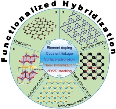
The discovery of graphene and subsequent verification of its unique properties have aroused great research interest to exploit diversified graphene-analogous 2D nanomaterials with fascinating physicochemical properties. Through either physical or chemical doping, linkage, adsorption, and hybridization with other functional species into or onto them, more novel/improved properties are readily created to extend/expand their functionalities and further achieve great performance. Here, various functionalized hybridizations by using different types of 2D nanomaterials are overviewed systematically with emphasis on their interaction formats (e.g., in-plane or inter plane), synergistic properties, and enhanced applications. As the most intensely investigated 2D materials in the post-graphene era, transition metal dichalcogenide nanosheets are comprehensively investigated through their element doping, physical/chemical functionalization, and nanohybridization. Meanwhile, representative hybrids with more types of nanosheets are also presented to understand their unique surface structures and address the special requirements for better applications. More excitingly, the van der Waals heterostructures of diverse 2D materials are specifically summarized to add more functionality or flexibility into 2D material systems. Finally, the current research status and faced challenges are discussed properly and several perspectives are elaborately given to accelerate the rational fabrication of varied and talented 2D hybrids.

Keywords: 2D nanomaterials; functionalization; heterostructures; hybrid; modification.


Conflict of interest statement

The authors declare no conflict of interest.

Figures

Figure 1
Figure 1
Functionalized hybridization of various 2D nanomaterials via diverse strategies to combine different species.
Figure 2
Figure 2
a–c) Schematic strategies for top‐down production of 2D nanomaterials. a) Mechanical cleavage by using Scotch tape. Reproduced with permission.37 Copyright 2012, Institute of Physics. b) Sonication‐driven exfoliation via 1) the addition of exfoliating/stabilizing agents, 2) sonication, and 3) increment of sonication time. Reproduced with permission.38 Copyright 2014, American Chemical Society. c) Ion intercalation‐assisted exfoliation. Reproduced with permission.39 Copyright 2018, The Royal Society of Chemistry. d) Schematic strategies for bottom‐up production of 2D nanomaterials: hydrothermal and solvothermal synthesis of MoS2 nanosheets. Reproduced with permission.43 Copyright 2015, The Royal Society of Chemistry; and with permission.5 Copyright 2011, American Chemical Society. e) Chemical vapor deposition of WS2 nanosheets. Reproduced with permission.44 Copyright 2013, American Chemical Society.
Figure 3
Figure 3
Element doping of TMD layers. a) Schematic doping of various ions and atoms into/onto MoS2 layers. b) Phase engineering of MoS2 nanosheet after intercalated by Li+ or Na+. Reproduced with permission.54 Copyright 2015, American Chemical Society; and with permission.55 Copyright 2014, American Chemical Society. c) TiS2 nanosheet doped with H. Reproduced with permission.58 Copyright 2013, American Chemical Society. d) MoS2 nanosheet doped with O. Reproduced with permission.59 Copyright 2013, American Chemical Society.
Figure 4
Figure 4
Sulfur vacancy passivation by alkanethiol molecules. a) Schematic drawings of a MoS2 field effect transistor before and after the treatment with alkanethiol molecules. b) Raman spectra of sulfur vacancies. c) I DSV G curves before and after thiol treatment with logarithmic scale. The inset shows I DSV G curves with linear scale. Reproduced with permission.67 Copyright 2015, American Chemical Society.
Figure 5
Figure 5
C—S bonding‐mediated surface functionalization of MoS2 nanosheets. a) Schematic modification of MoS2 nanosheets with 2‐iodoacetamide or iodomethane. Reproduced with permission.69 Copyright 2014, Nature Publishing Group. b) Schematic basal‐plane functionalization of MoS2 with 4‐methoxyphenyldiazonium tetrafluoroborate. Reproduced with permission.70 Copyright 2015, American Chemical Society.
Figure 6
Figure 6
Noncovalent hybridization of BSA on MoS2 nanosheets. a) Schematic binding of BSA on MoS2 layer via benzene rings and disulfides. b) AFM image of single‐layer MoS2 bonded with BSA. c) Biocompatibility and d) specific capacitance of MoS2‐BSA nanosheets and other MoS2 products. As observed, the surface‐hybridized BSA endows a better biocompatibility and a larger specific capacitance due to its biological and insulative nature. Reproduced with permission.73 Copyright 2015, American Chemical Society.
Figure 7
Figure 7
Schematic illustration of BSA‐induced exfoliation of WSe2 nanosheets and then loading with photosensitizer methylene blue on nanosheets for synergistic photothermal/photodynamic cancer therapy. Reproduced with permission.99 Copyright 2017, The Royal Society of Chemistry.
Figure 8
Figure 8
Epitaxial growth of Au nanoparticles on MoS2 nanosheets by using BSA‐caged Au25 nanoclusters. a) Schematic exfoliation of MoS2 nanosheets and subsequent surface growth of Au25 clusters into Aum nanoparticles. b) Low‐resolution and c) high‐resolution TEM images of Aum/MoS2 nanosheets, and d) their enlarged TEM image from the highlighted area in (c). e) Schematic growth of Aum to Aum + n nanoparticles on MoS2 nanosheets with time upon the addition of H2O2, and the corresponding color evolution. Reproduced with permission.122 Copyright 2018, The Royal Society of Chemistry.
Figure 9
Figure 9
The hierarchical growth of MoS2 nanosheets on the inner surface of TiO2 nanocavities. a) Schematic illustration for the fabrication process of MoS2@TiO2 heterostructures. b) Top‐view SEM image, c) TEM image and d) high‐resolution TEM image of MoS2@TiO2 heterostructure with a MoS2 thickness of 10 nm. e) Schematic diagram of the energy band structure, plasmonic resonance, and electron transfer pathway in the MoS2@TiO2 heterojunction. Reproduced with permission.129 Copyright 2018, The Royal Society of Chemistry.
Figure 10
Figure 10
Graphene growth along Zigzag (z) and Klein (k) edges on Ni(111). a) Zigzag and Klein edges of a top‐fcc epitaxial graphene layer. b,c) High‐speed scanning tunneling microscopy acquired in quasi‐constant height mode at the z edge b) and the k edge c). White arrows indicate the position of C atoms in fcc‐hollow sites near the kink. Reproduced with permission.143 Copyright 2018, Science.
Figure 11
Figure 11
Hybridization of metal oxides on RGO nanosheets. a) Schematic representation of the sol–gel strategy toward ultradispersed TiO2 nanocrystals on graphene. HRTEM image (right) showing nanosized TiO2 with highly exposed edges stacked on graphene nanosheets. Reproduced with permission.153 Copyright 2013, American Chemical Society. b) Schematic processes for synthesizing the hybrid of graphene and phosphorized SnO2. Reproduced with permission.160 Copyright 2018, The Royal Society of Chemistry.
Figure 12
Figure 12
The growth of W18O49 nanograsses on g‐C3N4 nanosheets. a) Synthetic approach to W18O49/g‐C3N4 heterostructure. b) SEM images of top and side view of the heterostructure. c) TEM image and the corresponding elemental mapping images of the heterostructure. Reproduced with permission.175 Copyright 2017, Wiley‐VCH.
Figure 13
Figure 13
Chemical passivation of BP layers via covalent modification. a) Reaction scheme of benzene‐diazonium tetrafluoroborate derivatives on BP layer. b,c) AFM characterization and d) histograms of the surface roughness of pristine BP flake immediately after exfoliation and after ten days of ambient exposure. e,f) AFM characterization and g) histograms of the surface roughness of the BP morphology immediately after functionalization with 4‐nitrobenzene‐diazonium (4‐NBD) for 30 min and after ambient exposure for ten days. Scale bars are 2 µm. Reproduced with permission.190 Copyright 2016, Nature Publishing Group.
Figure 14
Figure 14
The selective growth of Co2P nanocrystals on the BP edges. a) TEM image of one BP/Co2P nanosheet. b) HR‐TEM image of Co2P corresponding to the edge location and c) HR‐TEM image of BP corresponding to the center position. d) AFM image and line‐scan of one BP/Co2P nanosheet. e) Schematic synthesis of BP/Co2P heterostructures. Reproduced with permission.205 Copyright 2018, Wiley‐VCH.
Figure 15
Figure 15
Controlled exfoliation of WO3 nanosheets in a pH 4 solution and subsequent hole creation on resulting nanosheets in a pH 8 solution. a) Schematic illustration for the electrostatic binding of BSA on WO3 surface. b) Calculated binding energies. c) High‐resolution TEM images of WO3 nanosheets. Reproduced with permission.42 Copyright 2017, Wiley‐VCH. d) Schematic illustration from the WO3 bulk to WO3 nanosheets to porous nanosheets. e) pH‐dependent evolution of the absorption intensity of WO4 2− ions after WO3 powder is dissolved in aqueous solutions at different pH values for 24 h. f) TEM image of porous WO3 nanosheets and the comparison on catalytic ability of different samples (inset). Reproduced with permission.216 Copyright 2018, American Chemical Society.
Figure 16
Figure 16
Chemical synthesis of Pt‐SnO2 nanosheets. a) Schematic illustration of synthetic process. b) TEM image of SnO2 nanosheets functionalized by Pt nanoparticles. c) High resolution TEM image of Pt‐SnO2 nanosheets. Reproduced with permission.219 Copyright 2018, Wiley‐VCH.
Figure 17
Figure 17
Hybridization of different TMD nanosheets. a) Schematic of lateral epitaxial growth of WS2–WSe2 heterostructures. b) AFM image of WS2–WSe2 lateral heterostructure. Inset is optical image of a triangular domain. Scale bars = 5 µm. c) Raman and d) photoluminescence characterization in the center region and the peripheral region of WS2–WSe2 heterostructures: 1,2) are Raman mapping at 419 and 256 cm−1, respectively; 3,4) are photoluminescence mapping at 665 and 775 nm, respectively. Reproduced with permission.236 Copyright 2014, Nature Publishing Group. e) SEM image of the ternary MoS2 xSe2(1− x ) nanosheets (x = 0.48). f) Normalized photoluminescence spectra of the MoS2 xSe2(1− x ) nanosheets excited with a 488 nm argon ion laser. Curves (a–l) are the MoS2 xSe2(1− x ) nanosheets synthesized at temperature of 830 to 796 °C, respectively. Reproduced with permission.238 Copyright 2014, American Chemical Society.
Figure 18
Figure 18
a) Schematic illustration for synthesizing sandwiched VG/MoSe2/N‐C core/shell arrays and b–d) SEM images of typical products. VG represents vertical graphene and N‐C represents N‐doped carbon in shell. Reproduced with permission.250 Copyright 2017, Wiley‐VCH.
Figure 19
Figure 19
A van der Waals heterojunction p–n diode based on BP and MoS2 nanosheets. a) Schematic device structure. b) Optical image of device structure. The dark purple region is monolayer MoS2 while the blue flake is few‐layer BP. Scale bar, 10 µm. c) Gate tunable IV characteristics of the p–n diode. The top inset shows the IV characteristics under semilog scale. The bottom inset shows the rectification ratio as a function of back gate voltage V g. Reproduced with permission.254 Copyright 2014, American Chemical Society.
Figure 20
Figure 20
Surface hybridization of WO3 and MoS2 nanosheets into WO3/MoS2 hybrid by simultaneously exfoliating them in the presence of BSA. a) Schematic formation for WO3/MoS2 nanosheet sandwiched with BSA. b) Low‐resolution TEM image of a WO3/MoS2 hybrid prepared at the weight ratio of WO3/MoS2 = 4:1, accompanied with the high‐resolution TEM images on its individual nanosheets. Reproduced with permission.42 Copyright 2017, Wiley‐VCH.

Similar articles

Cited by

References

    1. Novoselov K. S., Geim A. K., Morozov S. V., Jiang D., Zhang Y., Dubonos S. V., Grigorieva I. V., Firsov A. A., Science 2004, 306, 666. - PubMed
    1. Novoselov K. S., Jiang D., Schedin F., Booth T. J., Khotkevich V. V., Morozov S. V., Geim A. K., Proc. Natl. Acad. Sci. USA 2005, 102, 10451. - PMC - PubMed
    1. Nicolosi V., Chhowalla M., Kanatzidis M. G., Strano M. S., Coleman J. N., Science 2013, 340, 1226419.
    1. Geim A. K., Novoselov K. S., Nat. Mater. 2007, 6, 183. - PubMed
    1. Altavilla C., Sarno M., Ciambelli P., Chem. Mater. 2011, 23, 3879.

LinkOut - more resources